
Understanding Blind and Buried Via Technology in PCBs
In the ever-evolving field of printed circuit boards (PCBs), blind and buried via technology has emerged as a revolutionary innovation, enabling the creation of more compact and high-performance electronic devices. Let's take an in-depth look at what these vias are, their working principles, advantages, applications, and the latest industry trends.
What are Blind Vias and Buried Vias?
Blind Vias
Blind vias are copper-plated holes that connect one outer layer of a PCB to one or more inner layers without penetrating the entire board. They can be regarded as shortcuts for electrical signals, allowing surface components to communicate efficiently with internal circuits. Blind vias are typically created using laser drilling, a high-precision method capable of producing holes as small as 0.1mm in diameter. For example, in a smartphone's PCB, blind vias enable the connection between outer-layer components (such as touchscreen controllers) and inner-layer power management circuits, making full use of limited space.
Buried Vias
Buried vias, on the other hand, are completely hidden inside the PCB, connecting two or more inner layers without being exposed on the outer surfaces. They are formed during the lamination process of PCB manufacturing. In the motherboard of a data server, buried vias play a crucial role in establishing connections between different layers of high-speed data processing circuits. Since they do not interfere with outer-layer components or traces, they provide a neat and efficient way to manage complex internal wiring.
Advantages of Blind and Buried Vias
Space Optimization
In the era of miniaturized electronic devices, every square millimeter on a PCB is of great importance. Compared with traditional through-holes, blind and buried vias significantly reduce the area occupied by vias. By eliminating the need for vias to penetrate the entire circuit board, more surface area is available for component placement. This is particularly critical in wearable devices, where the PCB must be small enough to be worn comfortably while integrating multiple functions.
Enhanced Signal Integrity
For high-speed and high-frequency applications such as 5G communication devices and advanced computing systems, signal integrity is paramount. Blind and buried vias provide shorter electrical paths, reducing signal loss, electromagnetic interference (EMI), and crosstalk. The shorter the path, the smaller the resistance and capacitance, ensuring that signals can be transmitted quickly and accurately. In 5G base station PCBs, these vias help maintain the integrity of high-frequency millimeter-wave signals, which is crucial for fast and reliable data transmission.
Design Flexibility
These vias offer designers greater flexibility in creating complex circuit layouts. Designers can use buried vias to isolate key circuits in inner layers while using outer layers for other wiring or component placement. This allows for better organization of the PCB's circuits, making it easier to manage power distribution, signal routing, and heat dissipation.
Practical Applications
Consumer Electronics
Blind and buried vias are widely used in smartphones, tablets, and smartwatches. They help integrate multiple functions into a small size. For example, in a smartwatch, blind vias connect the outer-layer display driver to the underlying processor and sensor interface circuits, while buried vias are responsible for internal communication between different functional modules of the processor.
Automotive Electronics
Modern cars rely heavily on electronic devices for functions such as autonomous driving, infotainment, and engine control. Blind and buried vias are used in automotive PCBs to ensure reliable and high-speed communication between various components. In autonomous driving radar systems, buried vias help route high-speed signals between different processing layers, while blind vias connect outer-layer sensors to inner-layer signal processing circuits.
High-Performance Computing
Data centers and high-performance computing systems require PCBs that can process large amounts of data at high speeds. Blind and buried vias are used in server motherboards to optimize signal routing and reduce interference, ensuring the smooth operation of processors, memory modules, and storage devices.
Industry Trends
Advances in Manufacturing Technology
Manufacturers are constantly improving the manufacturing processes of blind and buried vias. New laser drilling technologies are being developed to produce smaller and more precise vias. In addition, advancements in lamination processes allow for better control over the formation of buried vias, resulting in more reliable and higher-quality PCBs.
Integration with Other Technologies
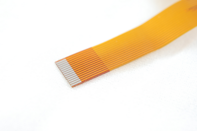
As the demand for smaller and more powerful electronic devices grows, blind and buried via technology is being integrated with other emerging technologies such as 3D-printed PCBs and flexible PCBs. In flexible PCBs used in foldable smartphones, blind and buried vias help maintain electrical connectivity when the device is bent or folded.
PCBgogo's Perspective
At PCBgogo, we recognize the importance of blind and buried via technology for the future of the electronics industry. Our advanced production facilities enable us to meet the complex manufacturing requirements of blind and buried via PCBs. Our team of experienced engineers is proficient in their design optimization and manufacturing. Whether for smartphones, automobiles, or high-performance computing, we can provide customized solutions based on customer needs. By keeping up with technology and investing in research and development, we ensure that our products meet high standards. Choose PCBgogo and let us help you realize your innovative ideas.

