Rigid-Flex PCBs – A Look At The Manufacturing Process by PCBGOGO
Introduction
You’ve heard of PCBs we bet, you know, those tiny green circuit boards with miniaturized electronics attached to the surface. If you’re looking into the PCB industry to have your PCBs manufactured you need to get the right info on which PCB would be more fitting for your product requirements.
You have plenty of options to go for; single layer, multi-layer, flexible, rigid, rigid-flex; but before you decide on anyone make sure you’ve done your research.
That’s what we’re here to help you out with! Read on to learn all you need about rigid-flex PCBs and where you can place your orders today!

Image Courtesy: pcbgogo.com
What is Rigid-Flex PCBs?
First things first, what exactly are rigid-flex PCBs?
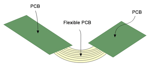
As the name suggests, these PCBs show a certain level of flexibility in their base. They incorporate both rigid and flexible PCB materials, making an amalgam of both. The final product will exhibit the advantages of both types of PCBs.
Usually, a rigid-flex PCB would be used in place of a rigid PCB where the addition of a sole rigid PCB would not be feasible. A single rigid-flex PCB can be constructed using multiple layers of flexible circuit bases attached to rigid PCB boards either externally or internally. The flexible PCBs are built to stay in a constant state of flex and so are built that way during manufacturing or installation, dependent of course on the applications you’ll be using it for.

Image Courtesy: pcbgogo.com
So how are rigid-flex PCBs created and how does the process differ from traditional rigid PCB manufacturing? The most contrasting difference is the types of materials used.
Rigid-Flex PCB Material Used
Rigid-Flex PCBs as we’ve mentioned before are used where rigid PCBs cannot. For example, in small shapes or fitted into shapes not possible for rigid PCBs. They are used in the military, medical and aerospace industries and even in smartphones, cameras and smart devices.
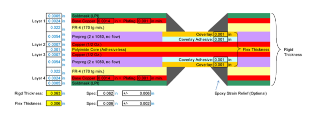
The IPC 2223C Sectional Design Standard for Flexible Printed Boards lists a few key elements for the design of a reliable rigid-flex PCB. These include the elimination or reduction of adhesive used in the rigid sections of the PCB, the use of adhesive-less based substrates, and the limited use of coverlay.
§ Reduction of Adhesive
Adhesives are used in making connections between the substrate and conductor materials. The adhesive used and the quantity of adhesive used can affect the service life of a PCB, hence why it is such as crucial part of rigid-flex PCB manufacturing.
Prior to the modern and evolves rigid-flex PCB design methods, many layers of adhesives were used in the rigid part of the PCBs. Adhesives tend to have a high coefficient of thermal expansion, much higher than that of FR-4 used in the substrate. Due to this in the events of thermal expansion during manufacturing cycles, there is a chance of cracks to form in the copper plating within via holes due to extreme stress on the vias.
This is why the use of adhesives needs to be reduced/limited.

Image Courtesy: pcbgogo.com
§ Use of Adhesive-less Based Substrate
In continuation of the reduction of adhesive used, manufacturers discovered a solution, the use of adhesive-less based substrate. Usually, copper layers are bonded to a polyimide core using an epoxy adhesive, in the case of an adhesive-less based substrate, the copper is directly attached to the polyimide core.
By eliminating the adhesive layer you can reduce the width and therefore get a more flexible design. This will help in reducing the overall stress on the vias making your design much more reliable.
§ Limited Coverlay
A coverlay or a coverfilm is used in flexible and rigid-flex PCB manufacturing to encapsulate and protect the circuit board. It acts similar to a solder mask used on a rigid PCB.
Prior methods of rigid-flex PCB manufacturing used coverlays that extended throughout the design. The coverlay adhesive used would then cause excessive stress during thermal expansion. To resolve this issue, coverlay is now limited to only the exposed flex areas.
With these three key elements, you’ll have a reliable rigid-flex PCB design that meets modern PCB standards.

Image Courtesy: pcbgogo.com
The Rigid-Flex PCB Manufacturing Process
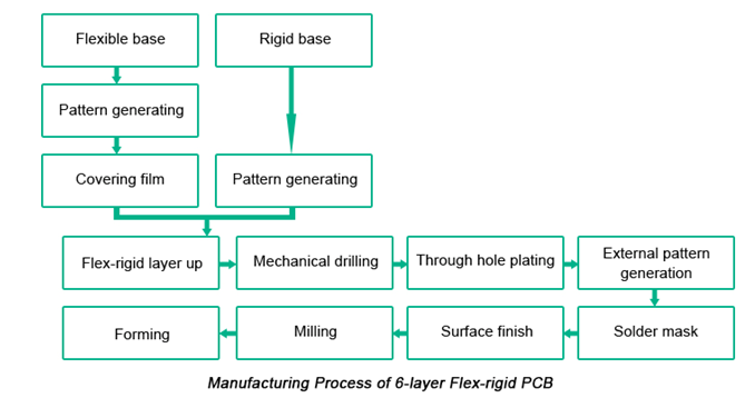
Now let’s speak about the actual rigid-flex PCB manufacturing process. We’ll go over the steps one by one.
§ Base Material Cleaning
First, you will have to clean your laminates for manufacturing. Your laminates include the cooper layers with adhesive. All laminates must be cleaned properly before you proceed with the rigid-flex PCB manufacturing process. This is a very important step in the process because cleaning will remove the antirust layer from the copper coil. This layer is usually added to help prevent oxidation but it is an obstacle in the rigid-flex manufacturing process and so it must be removed.
Usually, the copper foil is treated to an acid solution, then with a sodium persulfate solution, and finally coated with a more suitable oxidant.
§ Circuit Printing
Next, you will have to work on your circuit pattern. There are a number of ways to add the circuit pattern to your laminate. Some of the most common ones include screen printing and photographic imaging.
Screen printing is a technique in which a mesh is used to transfer ink onto a substrate through a stencil. Photographic imaging is a technique in which you place a photoresist film with the circuit pattern close to the laminate and then expose it to UV light. Finally, a chemical process will be used to remove the film so only the required circuit traces are left behind on the laminate.
§ Etching
Next, the copper laminate is etched. Usually, the rigid-flex PCB laminate will be immersed in an etching bath or sprayed with an etching solution to get the desired results. In order to get the best results, both sides of the copper laminate must be etched at the same time.
§ Drilling
The next step involves drilling. According to the design requirements drill holes, vias and pads. Usually, this process is automated using an automated PCB drilling machine.
§ Through-Hole Plating
The holes drilled into the PCB must then be plated with copper. The plated through holes will allow for connectivity between the conductive layers and components.
§ Coverlay/Coverfilm addition
Next, the top and bottom surfaces of the rigid-flex PCBs must be covered with a coverlay. This will help protect the final product from external factors.
§ Testing
The final step involves the testing and verification of the rigid-flex PCB. This step will help uncover any underlying errors in manufacturing and fabrication. This step will also ensure your final PCB is up to manufacturing standards. A flying probe test or X-ray inspection are some popular types used.

Image Courtesy: pcbgogo.com
That’s all, we’ve briefly discussed the rigid-flex PCB manufacturing process. In order to get more insight into the process, it is recommended to contact your designer.
PCBgogo is a manufacturer, located in Shenzhen, China. They offer rigid-flex PCB manufacturing at affordable costs without compromising quality.
Rigid-Flex PCBs – PCBgogo’s PCB Manufacturing Capabilities
Established in 2017 in Shenzhen, China, PCBgogo has established quite a foothold in the PCB manufacturing industry. PCBgogo offers PCB manufacturing and assembly services worldwide. It is RoHS and ISO 9001:2015 certified and claims to cater to over 100,000 clients worldwide and having delivered over $50 M worth of electronic components.
They are offering low-cost and affordable Flex and Rigid-Flex PCB manufacturing. You can order a complete customized quote from their website directly. You can also contact them atservice@pcbgogo.com to get the perfect PCB fabricated for your projects.
This article is originally published on electronicslovers.com and authorized to reprint on PCBgogo.
The original link: https://www.electronicslovers.com/2021/06/rigid-flex-pcbs-a-look-at-the-manufacturing-process-by-pcbgogo.html

