
Quality Control in PCB Manufacturing: A Simplified Guide to Full-Process Management
In the fast-paced electronics industry, PCBs are the backbone of devices from smartphones to aerospace systems. As demand for high-performance, miniaturized, and reliable PCBs grows, a comprehensive quality control (QC) system in manufacturing becomes essential.
1. Raw Material Inspection: The First Line of Defense
A PCB’s quality starts with raw materials—substrates (e.g., FR-4 for general use, PTFE for high-frequency), copper foils, and prepregs—all must meet strict standards (e.g., copper foil thickness uniformity affects conductivity). Reputable manufacturers source from trusted suppliers and conduct incoming checks: visual defect scans, dimensional tests, and electrical property checks. To combat counterfeits, X-ray fluorescence (XRF) analysis now verifies material composition.
2. Design Phase: Laying the Quality Foundation
Design is critical for PCB performance. With complex designs, Design for Manufacturing (DFM) principles are key—engineers use advanced software to optimize layout for signal integrity, power distribution, and thermal management (e.g., 5G devices need layouts to avoid signal distortion). Design for Testability (DFT) features are also integrated to simplify later testing.
3. Production Process Monitoring
3.1 Imaging and Etching
Laser imaging systems transfer circuit patterns to copper-clad substrates with high precision. During etching (removing excess copper to form traces), parameters like solution concentration, temperature, and time are strictly controlled—deviations cause short/open circuits.
3.2 Drilling and Plating
Precision drills (with auto-depth control) ensure accurate hole placement for component insertion. Holes are plated with copper for conductivity; plating thickness/uniformity is monitored in real time to avoid connection failures.
3.3 Soldering and Assembly
Surface-mount (SMT) and through-hole (THT) technologies attach components. Automated pick-and-place machines ensure accuracy; reflow/wave soldering uses precise temperature profiles to prevent bad solder joints. 3D solder paste inspection (SPI) before soldering catches printing defects.
4. Quality Inspection and Testing
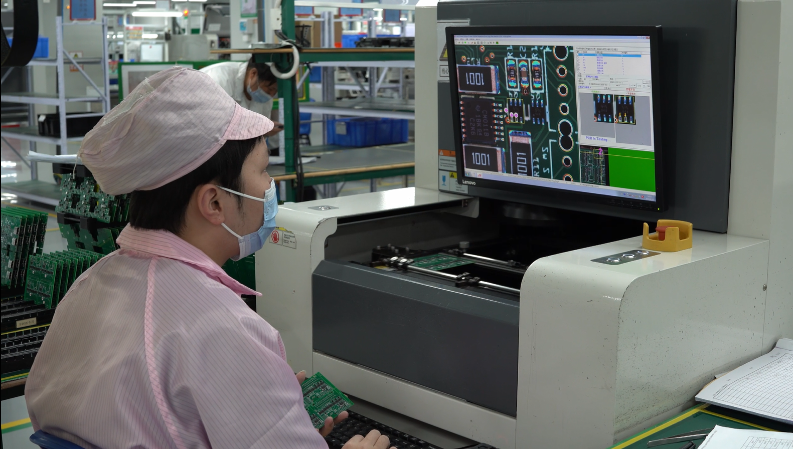
4.1 Automated Optical Inspection (AOI)
AOI uses high-res cameras and algorithms to scan for surface defects (missing components, solder bridges). Faster and more accurate than manual checks, it enables immediate rework.
4.2 X-Ray Inspection
Indispensable for hidden defects (e.g., BGA solder voids, multi-layer interconnection issues), X-rays penetrate PCBs to reveal internal structures.
4.3 Electrical Testing
In-circuit testing (ICT) checks for open/short circuits and component values; functional testing simulates real use. Automated test equipment (ATE) handles complex PCBs efficiently.
5. Industry Trends: AI and Data-Driven QC
AI-powered inspection systems learn from PCB image datasets to detect subtle defects. Predictive maintenance uses equipment data to reduce downtime. Manufacturing Execution Systems (MES) collect process data, helping manufacturers spot trends and optimize QC.
6. Conclusion: PCBgogo's Quality Commitment
At PCBgogo, we know quality comes from a well-planned QC system. From sourcing top materials to final inspection, every step ensures premium PCBs. We adopt AI and data-driven tools to improve QC, and our experienced team upholds high standards. By combining advanced tech with excellence, we meet customer needs and advance the PCB industry.

