PCB Routing Tips for Beginners
PCB routing
PCB design is a science as well as it is an art too. It is the technical work in which you should know about how to create a design, measurements, panel, width, and illustration. But once you know about it and know how to place all the components it will get interesting for you. PCB design consists of 90% placing and 10% routing. If the parts of PCB place correctly, at the end routing will be very easy and take less time. But it doesn’t mean that it is not important. There is not a specific way to place the parts of PCB because the placement of components is very flexible that makes the work very interesting and enjoyable. It is all the creativity you can do. But it doesn’t mean that you can do anything. The fact that the digital design you produce must be able to be created in its physical form remains a sobering reality. We all want to make a PCB design at a low rate and quickly, without any mistakes and trials. When it is time to manufacture the PCB design and convert your design into a circuit board, PCB design is more important at this time.
Importance of the placement of components
It is a very essential part of any PCB design because if components are not placed in the right place your design does not work in any case. It should be placed accurately because take the time in a perfect position it will make your whole life very easier when it's time to route everything and your circuit board will give its best performance. If you do not handle it with the care you will reveal that some parts have not space to be routed because they do not have enough space. The component placement jobs can result in the mainboard having to be rebuilt from the ground up. If the components are not wired correctly the board will not fit. Finally, you realize that your hard work and time are wasted. Anything from testing and usability to reliability and performance is impacted by PCB component placement. To provide electrical functionality, the circuits must be close to their linked components. The reality is that the preparation of PCB design plays a very important role in the results. The placement of the PCB parts directly affects the performance of the board. For thermal and mechanical requirements, the location of your components should be perfect. The improper position of the parts can cause soldering issues as well as major manufacturing roadblocks. It can cause the issues like a short circuit, power failure, and PCB inability. It may not be possible to resolve possible production problems in some cases, and you will have to restart the whole process from the beginning. It can affect every feature of PCB designs. These problems can be solved with proper guidelines and decisions during the PCB design. For that purpose, PCB designers especially beginners should follow the tips and rules before creating their ideas.
Tips for PCB routing
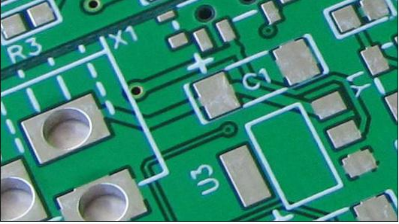
PCB routing is an art and creativity for the engineers. If you know how to work properly it will very enjoyable. For beginners here are some tips for routing the PCB that probably helps you to work easily and perfectly.

Image Courtesy: PCBgogo
10 Tips for PCB routing for beginners
Here we are discussing 10 tips that would help out you to routing PCB:
1. Familiar with your design specification
You should know that you must have the entire requirement you need to design the board before manufacture it. If you know about it you may set your trace size and space values in the design rules and later you prevent having to route again your whole design of the board. And by using this technique you will make your work easier.
2. Trace width
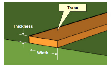
When electricity passes through all of the copper traces, it generates a significant amount of heat, which is often a problem in electronics. If you control the width of your trace it is one of the several ways to reduce the amount of heat that absorb on the surface. If the trace is wide the electricity can flow easily on the circuit because of less resistance. To know about the accurate size and trace’s thickness you can use a trace width calculator. It will help the users to access the estimated current and in return receive a value of trace width for internal and external layers.

Image Courtesy: PCBgogo
3. Do not depend on your auto-router
Automatic routing is called auto-router. When you use it the system chooses the right path of connection that you have select. It is an easy way to routing the board but it is never like self-routing. You can only use auto-routing when after you've placed all of your parts, you can use the auto-router to see what completion rating you receive. You will make changes in the position of your part if it is less than 85%. You can also use the auto-router to find difficult connection points that you might have missed during the component placement phase. Finally, you can use the auto-router to know how you may like to route any traces that you can't seem to finish. Apart from these three reasons never depend on your auto-router because it is not always correct. Furthermore, you can create your ideas and design them in your way and it will give better results. It is just creativity that demands more attention and care.
4. Make the distance between traces
When you layout the PCB board it is very important to leave enough space between all of the traces and sheets. Because if the traces are too near together the risk of a short circuit became high after you manufacture the board. For safety, experts recommended an almost 0.007” to 0.010” gap between the sheets and traces.
5. Do not use a 90-degree angle
During the process of PCB layout never use a 90-degree angle because when you have a group of traces on your board that makes a sharp right-angle turn, the outside corner of that 90-degree angle is likely to be marked narrow than your normal trace width. And at worst, you could get a lot of 90-degree traces back as the result. For that purpose try to use a 45-degree angle instead of a 90-degree so that it will create some beautiful design that makes your board perfect.
6. Space between traces and mounting gaps
During the process of place the parts of the components you should always place the space between gaps and traces. If you did not do this it might be a shock danger in the end. So always leave a ring space to secure the components while working with mounting holes.
7. Wide trace
All the traces of the PCB design board are the same so you have to make sure that the size of the trace is as wide as the path and power are. Because the current will have a flow more through the trace and path so if their size will not wide as an average of trace and path you'll get a lot of heat trying to get through those small gaps, which can burn wires and destroy your board. Try to not increase the heat in your board if there is any heating issue to deal with it find the component and dissolve the heat issue.
8. The same component must be in the same direction
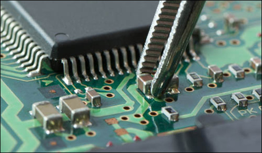
Try to align all of the components in the same direction in equally spaced rows or columns when working with groups of similar components. If you apply this technique it will be easy for you to insert, examine and check all of the parts you put on the board. This is important when dealing with Surface Mount Devices (SMDs) that are soldered using a wave soldering process. The bottom of your board will pass over a melted wave of solder during this wave soldering process, and any exposed metal pieces will be coated with solder when the wave hits them. As the wave solder passes over two exposed metal surfaces, such as a lead in a hole, a solder joint is created, allowing an electrical link to flow between your board and part. If these connections are not wired correctly, your board will end up with a lot of shorts and open circuits.

Image Courtesy: PCBgogo
9. Edge of the parts
Place all of the components that can't travel due to a mechanical system first, such as cables, switches, knobs, USB ports, and so on... You'll give yourself a great starting point for how your board layout needs to unfold to fit all of your input and output connections if you place these edge components first. After you have secured these edge components in place, you can get down to business with your interior parts.
10. Keep components on one layer
We always recommend putting all of your parts on the top layer when operating with a simple two-layer board. Making a physical PCB is a time-taking and costly operation, particularly if you end up putting components on the top and bottom layers. If you placed all of your components on the top layer of your board, this method is simple and will only require one pass through the pick-and-place machine. However, if you start putting pieces on your bottom sheet, you'll need to run it through the pick-and-place system again, which will add to your production costs.
Get your PCB routing services done at PCBgogo at affordable rates. Contact us at service@pcbgogo.com

