PCBGOGO SMT Assembly Process Explained
SMT is a revolutionary field electronic assembly that allows electronic components mounted on PCB surfaces. It is and contradicts technology to holes components embedding. Surface mount technology is used extensively for electronic module assembly reducing cost and gerent high-quality product. Almost all modern electronic devices made through surface mount technology.
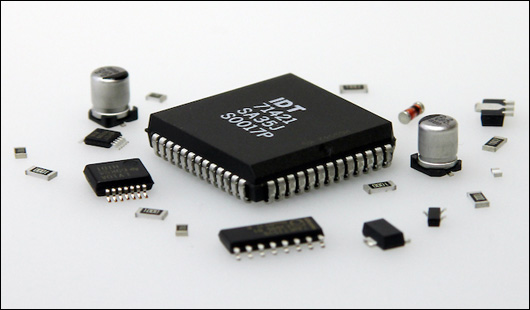
Image courtesy: PCBGOGO
SMT Assembly Process:
Welding technology and hole embedding have been replaced by SMT and all electronic industries are using this technology assembly process to manufacture PCB like computers, smartphones, telecommunication, and household appliances. Generally, the SMT assembly process comprised of Printing solder paste, components mounting, reflow soldering, AXI, or AOI testing.
Process 1- Feeder Loading:
Surface mount components placed on the board are being loaded by the feeder loading process. To conserve component size and consistency component of one type is loaded on each feeder.
Process 2-Pick & Place Machine programming:
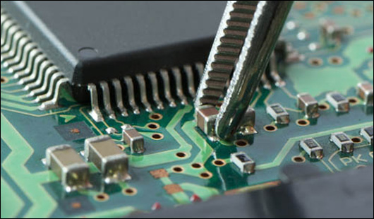
Pick and place machine is programmed as a second step. Location, orientation, and pad size of SMT components are programmed by Pick and Place files on the machine.
Process 3-Stencil Machine programming:
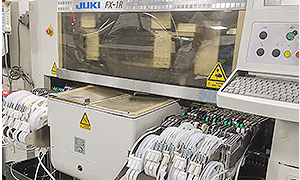
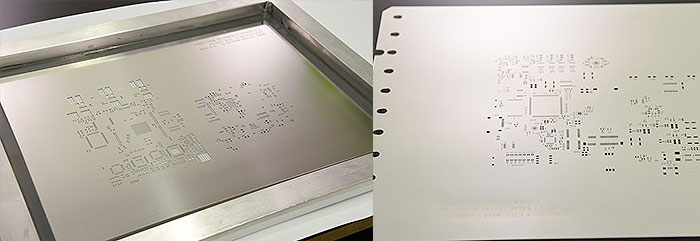
Stencils are widely used by PCB or electronic manufactures nowadays for solder paste printing which deposited on PCB board to assure the holding of each component in its place. In this way after reflow electronic components are secured on the PCB board. For the boards, the stencil aligns with SMT pads ensured by stencil printer programming.
Process 4-Solder Paste Printing
After setting up the stencil printer, solder paste printing is done on the board by using stencils. Squeegee is used to squeeze solder paste from the board. Stencils are removed when the deposition of solder paste is completed. A temperature-controlled environment is used to keep the Boards.
Process 5-Pick and Place Machine:
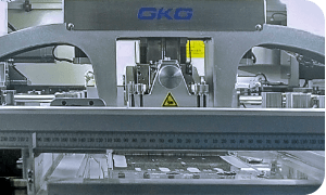
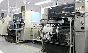
Boards are run through Pick and Place after paste printing is done. Nozzles are used to place components on the boards. This machine allows mounting of 20000 to 30000 components in an hour.
Process 6-Reflow Oven
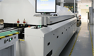
Boards coming through the pick and place machine directed to the oven for 5 to 7 minutes. In this process, the solder paste is reflowed and SMT components are completely soldered on the PCB boards. To attain the temperature of about 235 to 245°C RoHS amenable SAC305 solder paste is used.
Process 7-AOI testing machine
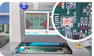
To check and evaluate possible manufacturing faults in PCB boards using SMT processing AOI (Automated Optical Inspection) is used. It can administer drawbacks like dimensional defects, placement of component defects, and surface defects, etc. Various algorithms are programmed in AOI machine-based proficiency to evaluate and differentiate standard PCB boards’ properties from defective boards.
AXI (Automated X-ray Inspection) along with AOI used to infer the data for possible errors fixation, overcome the defects, and boards efficiency optimization to make the high-quality final product.
SMT assembly benefits:
Surface mount technology was acquired to minimize the cost spent for manufacturing the boards and provides efficient and versatile usage of PCB. A higher level of automation used in SMT processing allows developing smaller assemblies having excellent repeatability for highly complicated electronic circuits.
§ Lightweight and smaller in size:
PCB weight and size can be reduced into smaller and accessible formations using surface mount technology components assembly on the PCB boards. SMT proposed assembly process allows placing more components in confined space on boards. Through this technique compact and complex designed having high efficiency can be achieved.
§ High liableness:
After prototype confirmation, all SMT assembly processes are automatic through programmed machinery that allows error reduction from manual processing. PCB boards and functioning are more consistent and reliable due to automation in SMT processing.
§ Budget-saving
As mentioned before SMT processing rely on automatic machinery that provides so many benefits in processing reliability and efficiency but at the same time, input cost for the machinery is high. Automatically programmed machines minimized the manual workforce which tends to ameliorate production quality and efficiency along with the reduction in labor monetary value. The previously used conventional method of the Through-Hole assembly process tends to utilize more materials whereas SMT processing does not require so many materials and in this way, the cost tends to reduce too.
PCBGOGO providing capable SMT Assembly
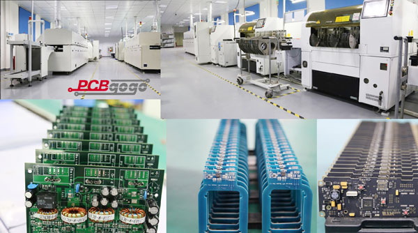
PCBGOGO possesses an entirely automatic and computerized SMT assembly workshop allowing mass production. Manual welding and processing services are also available for prototyping, minor batch orders, and complicated parts manufacturing. PCBGOGO owns several PCB types assembling like aluminum boards, rigid-flex boards, flex boards, and FR4 boards. Along with SMT assembly other types of assemblies like through-hole assembly, BGA assembly, kit assembly, and mixed assembly are also provided.
PCBGOGO bears a professional team of experts and engineers working for turnkey services of PCB orders. The team of engineers is specialized and expert in PCB manufacturing as well as SMT prototype. The components provided by the company or on customer’s demand, it is assumed that all the components and SMT assembly process are well checked and tested which efficiently match with your required design and request.![]()
This article is originally published on electronicslovers.com and authorized to reprint on PCBgogo.
The original link: https://www.electronicslovers.com/2021/04/pcbgogo-smt-assembly-process-explained.html
