How PCB Blind Vias "Stack Up": A Look at Any-Layer HDI Technology
In the world of high-performance electronics, compact design and blazing-fast data transfer are non-negotiable. To achieve this, engineers need to pack more components and traces onto a smaller board. This is where High-Density Interconnect (HDI) technology comes in, pushing the boundaries of what’s possible with PCB design.
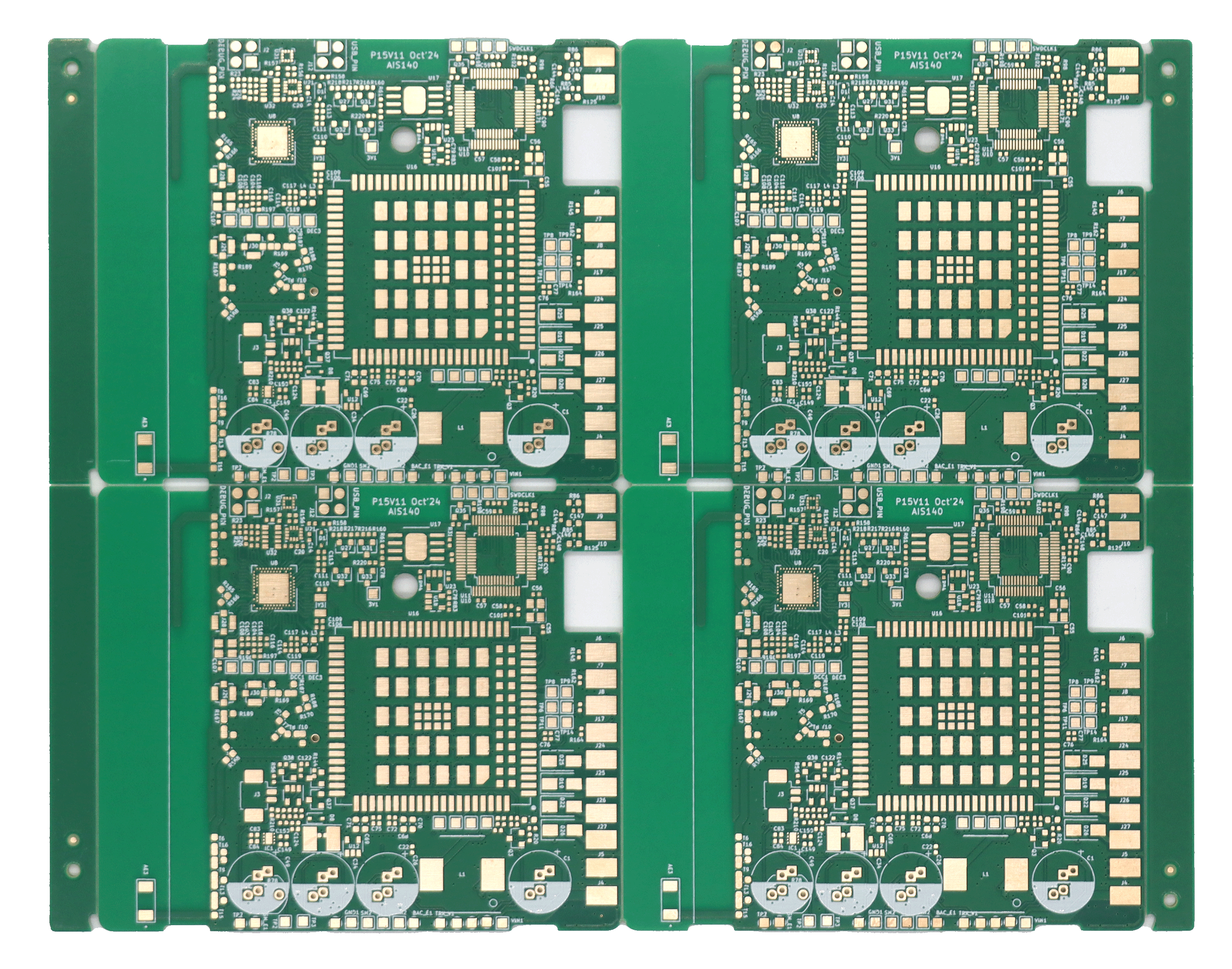
But as circuit complexity grows, a traditional HDI board with its nested, staggered blind vias can still present a challenge. The solution lies in a cutting-edge technique known as Any-Layer Interconnect, or "Any-Layer HDI." This technology allows blind vias to “stack up” on top of one another, dramatically increasing routing density and creating a true masterpiece of multi-level circuitry.
Understanding the Basics: From Through-Holes to Blind Vias
To appreciate Any-Layer technology, you first need to understand the evolution of vias.
Through-Holes: The simplest type of via, a through-hole extends from the top layer to the bottom layer, connecting all layers in between. They're reliable but take up valuable space on every layer they pass through, limiting routing options.
Blind Vias: An HDI board's signature feature, a blind via connects an outer layer to one or more inner layers without going all the way through the board. They are typically created with laser drilling. This method saves space on the layers they don't penetrate, allowing for denser routing.
While a significant improvement, conventional HDI boards still have a major limitation. To connect multiple layers, you often have to use a series of blind vias, but they must be "staggered" or offset from each other. They cannot stack directly on top of each other. This is because creating a reliable connection between stacked blind vias with traditional methods is extremely difficult, if not impossible. The need for staggering still consumes valuable real estate and adds complexity to the design process.

The Innovation of Any-Layer: A True "Stack-Up"
Any-Layer HDI technology overcomes the limitations of staggered vias by creating a reliable, stacked connection between blind vias. This is achieved through a combination of advanced manufacturing techniques:
Laser Drilling: Precisely drilling microvias layer by layer.
Conductive Paste & Planarization: After drilling, the vias are filled with a specialized conductive paste, then planarized (flattened) to create a perfectly flat surface for the next layer.
Advanced Plating: A subsequent plating process ensures a robust electrical connection between the filled via and the copper pad above it, allowing the next via to be "stacked" directly on top.
This process is repeated for each layer, creating a vertical series of connected blind vias—a true "stack-up." The result is a board with unprecedented routing freedom. You can now connect any two layers of the board directly, without the need for a staggered path or a through-hole.
The Impact on Modern Electronics: The Age of Miniaturization
The ability to create stacked vias is a game-changer for high-end electronics:
Miniaturization: Any-Layer HDI is a key enabler for miniaturizing devices. By stacking vias, engineers can reduce the board's footprint while maintaining, or even increasing, functionality. This is crucial for products like smartphones, smartwatches, and medical wearables.
Enhanced Signal Integrity: Stacked vias create a more direct and shorter path for signals, minimizing impedance changes and signal loss. This is essential for high-speed data transmission in technologies like 5G and AI processors, where every millimeter of trace length can affect performance.
Thermal Management: The stacked vias themselves act as effective thermal pathways, helping to dissipate heat from high-power components. This is a significant advantage for dense, power-hungry boards found in servers and high-performance computing.
The proliferation of Any-Layer HDI is a clear trend in the industry, driven by the demand for higher performance in a smaller form factor. Major players in the consumer electronics and telecom industries are rapidly adopting this technology, recognizing its role in meeting the challenges of tomorrow's devices.
Our Perspective at PCBgogo
At PCBgogo, we have always been at the forefront of advanced PCB manufacturing. We understand that our clients’ most ambitious designs require capabilities that go beyond the conventional. That's why we’ve heavily invested in the equipment and expertise to master Any-Layer HDI technology.
We are proud to offer this capability, allowing our customers to push their designs to the absolute limit. We believe that by providing this kind of cutting-edge technology, we can empower you to create smaller, faster, and more powerful products. We're not just a manufacturer; we're a partner dedicated to turning your most complex ideas into reality, layer by layer, with the precision and reliability that your projects demand.

