The global push for carbon neutrality has turned "green manufacturing" from a buzzword into a survival imperative for the PCB industry. Known for its reliance on chemicals, energy, and water, PCB production faces growing pressure—stricter regulations (like EU’s REACH and China’s "Double Carbon" policies) clash with the need for fast turnaround and cost control. So how do we reconcile these two? It starts with reimagining every step of the process.
Traditional PCB materials often contain lead, brominated flame retardants, and volatile organic compounds (VOCs). Today, alternatives are changing the game:
Lead-free laminates: Replacing lead-based solders with tin-silver-copper alloys wasn’t easy—early versions had poor thermal stability. Now, advanced formulations meet RoHS standards while matching the reliability of old materials, crucial for automotive and medical PCBs where durability is non-negotiable.
Recycled substrates: Companies like Japan’s JDI are using recycled glass fiber in PCB substrates, cutting raw material use by 30% without compromising mechanical strength. It’s not just eco-friendly; it reduces dependency on virgin resources, stabilizing costs.
Efficiency and eco-friendliness converge when processes are redesigned to minimize waste:
Closed-loop water systems: PCB etching uses toxic chemicals like ferric chloride, and wastewater used to be a major pollutant. Modern plants now recycle 90% of process water through filtration and ion exchange—slashing water usage by 70% while lowering disposal costs. A mid-sized factory can save $500,000 yearly with such systems.
Energy-smart factories: Switching to solar-powered workshops and variable-frequency drives for machinery reduces carbon footprints. In Taiwan, some PCB makers have cut energy consumption by 15% by optimizing production schedules to avoid peak-hour electricity surcharges—proving green practices can boost margins.
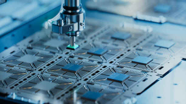
The rise of Industry 4.0 offers a third way: using data to eliminate inefficiencies that harm both the planet and profits.
AI-driven process control: Machine learning algorithms monitor etching times and chemical concentrations in real time, preventing over-etching (which wastes materials) or under-etching (which requires rework). This has cut scrap rates from 8% to 3% at leading factories.
Digital twins: Simulating PCB designs virtually before production helps identify material-heavy layouts. For example, optimizing layer stacking via 3D modeling can reduce copper usage by 10% per board—saving resources while speeding up prototyping.
Sustainability doesn’t end when a PCB leaves the factory. The industry is finally tackling e-waste:
Urban mining: Companies like Umicore extract gold, copper, and palladium from discarded PCBs using hydrometallurgical processes—recovering 95% of valuable metals, which are then reused in new boards. This reduces reliance on mining, which emits 10x more CO2 than recycling.
Design for disassembly: Making PCBs with fewer adhesives and standardized components eases recycling. European automakers now require suppliers to use "easy-peel" laminates, ensuring PCBs from retired EVs can be efficiently stripped and recycled.
At PCBgogo, we’ve learned that green manufacturing isn’t a trade-off—it’s a mindset. We’ve invested in lead-free production lines that slash harmful emissions by 40% while maintaining 24-hour prototyping speeds. Our AI-optimized etching processes reduce chemical waste, and we partner with recyclers to ensure our offcuts find new life. For us, balancing eco-friendliness and efficiency isn’t just about meeting regulations; it’s about building a industry that can thrive for decades. After all, the most efficient PCB is one that leaves the planet better than it found it.


