Introduction:
PCBs are an integral part of electronics, forming a major part of electric and electronic devices; therefore, having the fundamental knowledge of their concepts and basic terminologies is also integral. Here we will discuss a few basic definitions and concepts regarding printed circuit boards.
What is a Printed Circuit Board?
Contents
· 1 What is a Printed Circuit Board?
· 2 Soldermask
· 3 Silkscreen/Overlay
· 4 Layer Stackup
· 5 Types of Components
· 6 VIA (Vertical Interconnect Access)
· 7 PCBGOGO: One of the leading PCB manufacturers in China
A Printed Circuit Board or a PCB is a board containing lines and pads used to connect points on a circuit together. Traces are used to form electrical interconnections between various connectors and components.
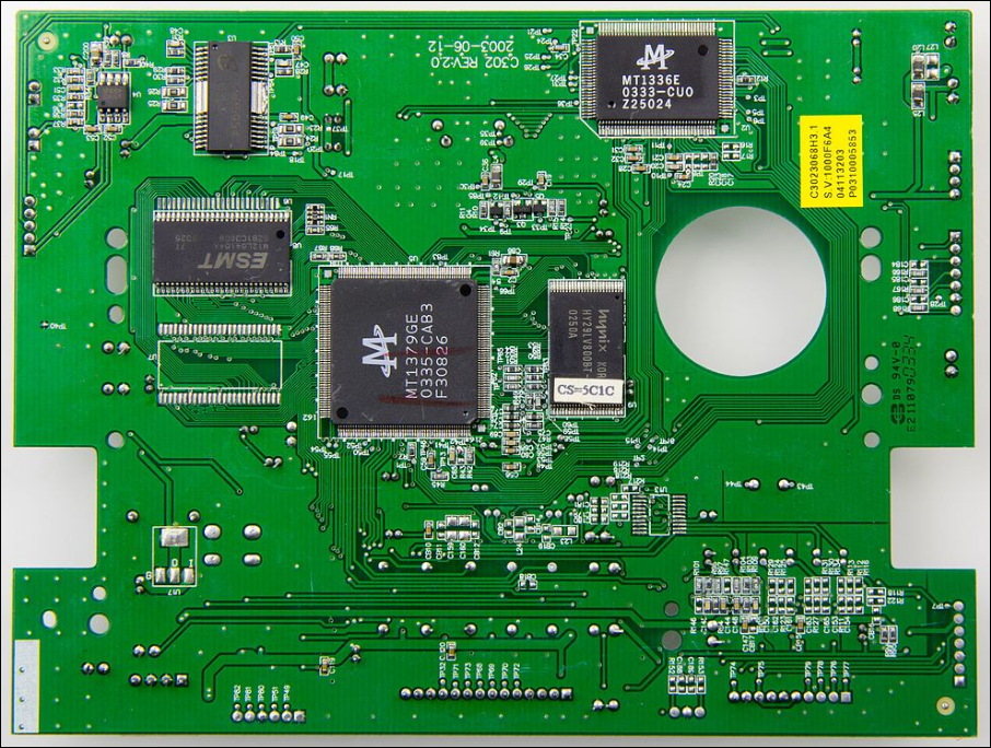
PCB of a DVD player. Typical PCBs are green, but they may also be made in different colors.Image Courtesy: CC BY-SA 4.0
The simplest type of PCBs contains copper traces that interconnect components of the PCB only on the surface, also commonly known as 1 layer PCBs. PCBs can also have more than one layers, 2 layer PCBs have traces on both the top and bottom layer, the more layers a PCB has the more complex its physical design will be.
Next, we will discuss some common terminologies affiliated with printed circuit boards i.e. solder mask, silkscreen/overlay, PCB layer stack-ups, thru-hole, SMD/SMT, BGA, pads, copper tracks, vias + its types.
Soldermask
Soldermask/ solder resist is a thin protective layer of polymer that is applied as a finish or varnish to the solder of printed circuit boards, on both top and bottom sides to prevent it from oxidation and short-circuiting. Soldermask is traditionally available in green color but is now available in a number of colors including red and blue. For example, PCBgogo, a PCB manufacturing firm in China offers solder masking services in a number of colors including green, red, blue. Yellow, white, matte black, purple and matte green, etc.
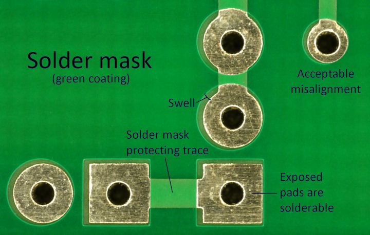
Image Courtesy: pcbgogo.com
Silkscreen/Overlay
Silkscreening allows the manufacturer to print any necessary information, logos, symbols onto the solder mask to help identify components, facilitate assembly and repair. Essentially, it is a layer of non-conductive epoxy ink traces applied to the components part of the PCB (sometimes silkscreen may also be applied to the solder of PCB but it will cost you more). The silkscreen is used to help indicate the test points, position, orientation, and test points of electronic components.
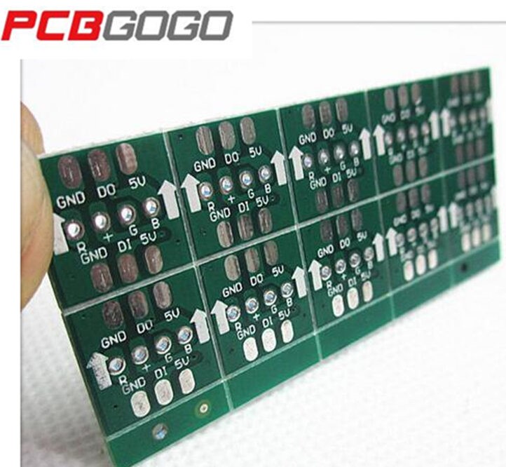
Image Courtesy: pcbgogo.com
Silkscreen can be printed on both sides of the board. You’ll commonly see silkscreen in black, white, and yellow colors. Two common silkscreen printing techniques you’ll find in use today include LPI (Liquid Photo Imaging) and DLP (Direct Legend Printing).
Layer Stackup
We’ve mentioned before that PCBs can be manufactured using multiple layers, Before a PCB board layout is designed, a layer stack-up is formed. A stackup is an arrangement of copper layers along with insulating layers that make up a PCB.
Layer stack-ups are important because while designing PCBs with the help of EDA software, layers specified may not always be conductive type (silkscreen, solder mask layers, etc.) Therefore, both conductive and non-conductive layers may cause confusion for manufacturers.
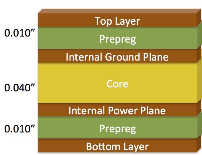
Standard 4-layer PCB stackup image courtesy:bitweenie.com
A good PCB layer stackup can also help reduce the circuits’ vulnerability to external noise and radiation effects and also optimize PCB designs for signal integrity, crosstalk, and electromagnetic interference.
Types of Components
We can classify the PCB components on the basis of the technology used to solder them onto the PCB. There are three basic types of electronic packages i.e. thru-hole, SMD/SMT, and BGA.
§ Thru-hole
Thru-hole technology is used for components having leads/pins that are mounted through plated holes into the PCB. They are then soldered to pads located on the opposite end of the PCB either manually or through automated machinery. According to PCBgogo, thru-hole technology is not only reliable but also more durable; “The through-hole assembly provides higher environmental stress because the components are held on the board by using leads inserting into the holes rather than simply being soldered on the PCBs’ surface as the SMT components. Thus, through-hole assembly offers a more robust physical connection, making it the preferred process for the military and aerospace industry that have high-reliability requirements.”
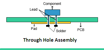
Image Courtesy: pcbdirectory.com
§ SMD/SMT
Surface Mount Devices or SMDs use Surface Mount technology for components that are mounted directly to the surface of PCBs. These types of components can be mounted onto both sides of the PCB. These components are usually smaller than those used in thru-hole technology.
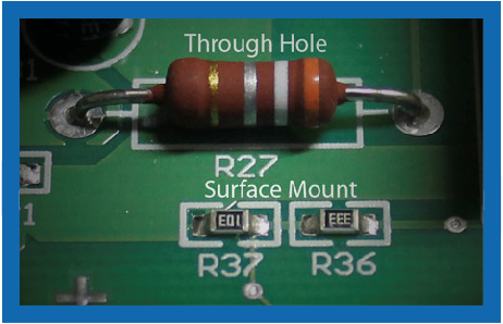
Image Courtesy: pcboardrework.com
§ BGA
A Ball Group Array is a type of surface-mount package used for ICs. The components in this category are used for high-density pin ICs. The pins on these components are made of solder balls which are then heated in the soldering process for making connections with the pads. Once the molten solder cools, it solidifies and holds the package with the circuit board.
Pads
Pads are small surfaces of copper in a PCB, these are surface areas designated for electrical contact where the components are soldered onto the PCB. Briefly, pads are exposed PCB surface parts where components are to be mounted/soldered. There are two main types of pads i.e. thru-hole and surface mount.
§ Thru-Hole Pads
Thru-hole pads are used where pins of the components are to be inserted into a PCB and soldered from the other end. Thru-hole pads may further be either plated or non-plated.
§ Surface Mount Pads
Surface Mount pads are used for surface mount devices where the component is to be soldered on the same surface.
Copper Tracks
A copper track is a conductive line or trace in a printed circuit board used to connect two points in the PCB, they may vary in length and width depending on the current which flows through them. Generally, power and ground traces are kept wider than signal traces.
VIA (Vertical Interconnect Access)
A VIA hole in a PCB consists of two pads on different layers of the same PCB which are connected through a hole made on the board. The hole is plated so as to assist in conducting current. It essentially allows the current to pass through the board.
Thru-Hole Vias
A via can be used to connect a component located on the top layer of PCB to another component located at the bottom layer. These types of vias are known as thru-hole vias.
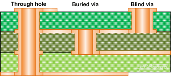
Image Courtesy: pcbgogo.com
Blind Vias
Blind Vias are used to form connections from an outer layer to an internal layer. Since it starts on an external later and ends in an internal layer we call it a ‘blind’ via. These types of vias are however more costly as compared to thru-hole vias.
Buried Vias
These types of vias are similar to blind vias, however, they connect two or more inner layers without going through any outer layer.
PCBGOGO: One of the leading PCB manufacturers in China
Located in Shenzhen, China, PCBgogo has established quite a foothold in the PCB manufacturing industry. PCBgogo offers PCB manufacturing and PCB assembly services worldwide. It is RoHS and ISO 9001:2015 certified and claims to cater to over 100,000 clients worldwide and has delivered over $50 M worth of electronic components.

Our products are proven to be reliable, worth the price they are delivered for plus we have astonishingly quick delivery times. We can deliver PCBs within 2-3 days or even faster depend on the urgency of your project. We deliver to countries all over the globe through services such as DHL, UPS, EMS, FedEx, and HK post, etc. You can also track the progress of your PCB assembly order and shipping status.
This article is originally published on electronicslovers.com and authorized to reprint on PCBgogo.
The original link: https://www.electronicslovers.com/2020/10/follow-these-key-factors-by-pcbgogo-before-moving-to-pcb-assembly-process.html
