
Building ‘Highways’ Finer Than a Hair: How PCB Circuits Are Made
When you look at a modern PCB, especially from a high-performance device like a smartphone or server motherboard, you’re seeing a marvel of micro-engineering. Some of the conductive lines on these boards are less than 3 mils (75 μm) wide—thinner than a human hair. How are these intricate “highways” built? As PCB professionals, we’re often asked this question. The answer lies in one of the most critical steps in PCB manufacturing: circuit formation.
Two primary methods are used to create these ultra-fine lines: the traditional subtractive method and the more advanced modified Semi-Additive Process (mSAP). Both have their roles in modern PCB production, especially as demand grows for higher density and smaller devices.
The Subtractive Method: Carving Out the Circuits
Think of the subtractive process like sculpting. You start with a full block of material and remove what you don’t need.
Process Flow:
It begins with a laminate core coated with a thin layer of copper. A photoresist layer is applied and then exposed to UV light through a patterned film. After development, the exposed copper is etched away using chemicals like alkaline ammonia, leaving behind the desired copper traces.Limitations:
As trace widths go below 3 mils, etching becomes challenging. The etching process is isotropic, meaning it removes copper not only vertically but also sideways—leading to undercutting and trapezoidal-shaped traces instead of rectangular ones. This affects impedance control and signal integrity in high-frequency designs.
2. The mSAP Method: Building Up, Not Cutting Away
For advanced boards such as IC substrates, smartphone motherboards, and high-speed server PCBs, the modified Semi-Additive Process (mSAP) is often the go-to choice. This method is additive—it builds up the circuit pattern instead of etching excess material away.
Process Flow:
A very thin layer of copper (usually < 3 μm) is deposited on the substrate.
A photoresist is applied and imaged with the circuit pattern.
Additional copper is electroplated only onto the exposed areas where traces are needed.
The photoresist is stripped away.
The original thin copper layer is etched away quickly, leaving only the thicker plated traces.
Why It’s Superior for HDI:
Since the traces are formed by plating, they have nearly vertical sidewalls, improving precision and impedance control. This allows line width/spacing down to 2/2 mil or even smaller—essential for today’s 5G, AI servers, and wearable electronics.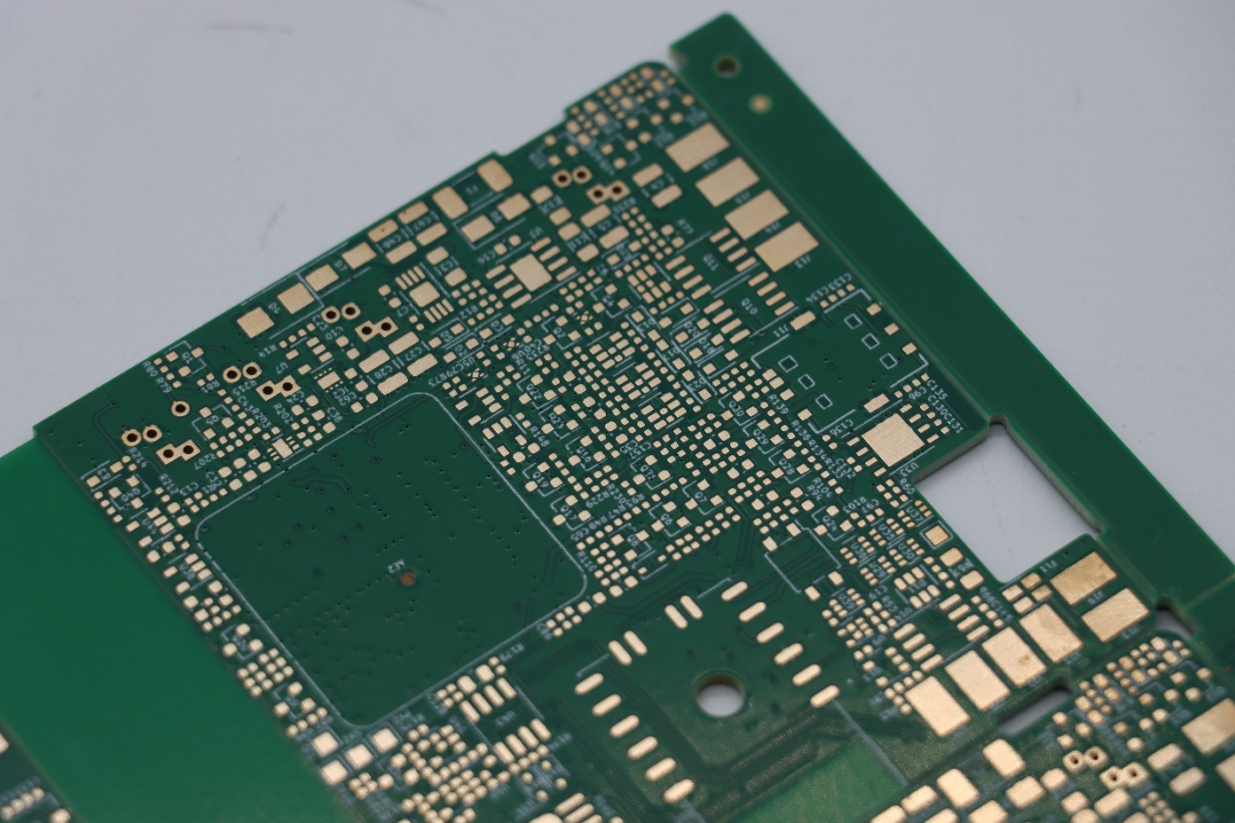
3. Why This Matters Today & Where the Industry Is Headed
The push for finer lines isn’t just about making smaller devices. It’s driven by higher functional density, increased signal speeds, and the need for improved thermal performance.
Trends Driving Adoption:
With the rollout of 5G and expansion of IoT, high-frequency materials and finer circuits are becoming standard. Advanced packaging technologies like SiP (System-in-Package) also rely on ultra-HDI PCBs made using processes like mSAP.Manufacturing Challenges:
tighter tolerances require more sophisticated equipment—laser direct imaging (LDI) to replace traditional phototools, superior plating chemistry, and highly automated optical inspection (AOI) systems.
Conclusion: At PCBgogo, We Build the Future, Line by Line
At PCBgogo, we’ve kept pace with these technological shifts. With over a decade of experience, we’ve incorporated advanced manufacturing techniques like mSAP and LDI to serve customers who demand high-reliability, high-density PCBs.
Whether it’s supporting innovation in 5G infrastructure, automotive electronics, or next-gen consumer gadgets, we understand that every micron matters. Our investment in modern equipment and strict process control ensures that even the finest circuits are built with precision and reliability.
We are more than a PCB manufacturer—we are your partner in navigating the complexities of modern electronics. Because when it comes to building the pathways of innovation, we believe there’s no room for compromise.

