An Introduction to High-Density Interconnect PCBs
Introduction
The PCB industry is always evolving, introducing new products and new technologies to combat the needs of the changing times. One such ‘evolution’ is the introduction of HDI PCBs, also known as High-Density Interconnect PCBs. If you’re a member of the industry or a simple PCB hobbyist, you need to get to know more about this PCB variant.
Here we’ll be discussing what HDI PCBs exactly are, what they do, their structure, and their various applications.
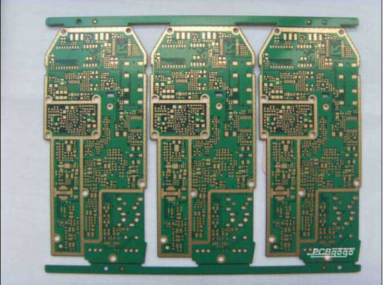
Image Courtesy: pcbgogo.com
What are HDI PCBs?
High-Density Interconnect PCBs are simply a type of PCB with a higher number of interconnections, which in turn leads to lesser space consumed. Hence giving you a miniaturized circuit board. The components are placed closer together all without compromising the performance of the PCB.
While ordinary PCBs cannot accommodate all components in smaller circuit areas, HDI PCBs allow the manufacturer to fit more technology in lesser space. All done through a combination of micro-vias, blind vias, via-in-pads to name a few which help utilize the given space as efficiently as possible.
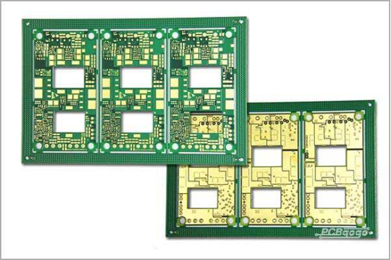
Image Courtesy: pcbgogo.com
Structure of an HDI PCB
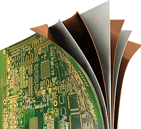
As for the structure of HDI PCBs, these are multi-layer boards whose layers are more densely populated with lines and copper routing. There are various vias used throughout the PCB stack-up which allow the layers to be electrically interconnected. The entire board itself is held together through a lamination process.
First, the inner copper layers are etched, then they are separated by partially cured laminates. They are then stacked with layers of prepreg on the top and bottom. The entire stackup is subjected to heat so the prepreg is liquified. Once the prepreg cools down it solidifies and the stackup is now held together. In the case of blind and buried and blind vias, the PCB will undergo several laminations, however, this will also increase the cost of the board.
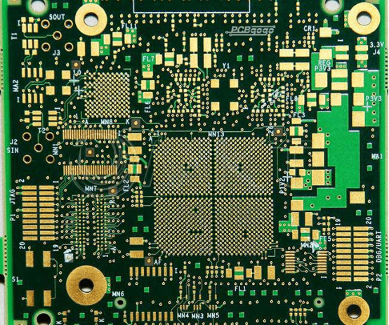
Image Courtesy: pcbgogo.com
HDI PCBs vs. Standard PCBs
There are a number of key differences between traditional PCBs and HDI PCBs. For one, HDI PCBs have more densely routed layers making their density greater as opposed to traditional PCBs.
HDI PCBs are also much smaller and lighter when it comes to circuit board size and weight, on the other hand, standard PCBs are much larger and heavier. As for the use of vias, HDI PCBs will incorporate blind vias, micro-vias, and buried vias in their stackup whereas standard PCBs use through-hole vias, blind vias, and buried vias. HDI PCBs are also compatible with higher pin count devices and small pitch devices as opposed to standard PCBs which are not always compatible.
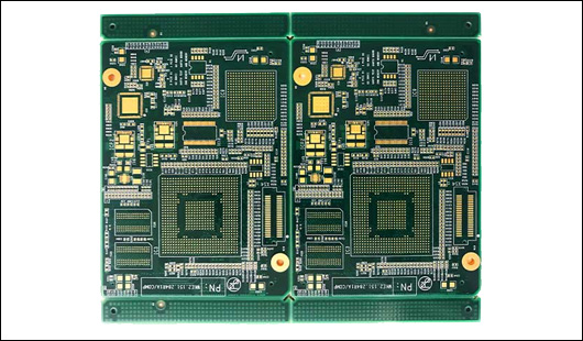
Image Courtesy: pcbgogo.com
Types of HDI PCBs
Based on the IPC-2315 standards, we can identify 3 main types of HDI PCBs i.e. Type I, Type II and Type III
§ Type I
This type of HDI PCB comes with a laminated core and makes use of a printed through hole (PTH) for interconnectivity. You will also find a single microvia layer on either one side of the laminate core or both. However, it lacks buried vias in its stackup.
§ Type II
This type of HDI PCB comes with a sequentially laminated core and makes use of a single microvia layer on one or both sides of the core. It does however come with both microvias and PTH for interconnectivity and blind along with buried vias.
§ Type III
The type III structure consists of a laminate core with microvias on either one or both sides of the PCB, it also makes use of blind and buried vias. The manufacturer may use both staggered and stacked microvias.
Applications of HDI
§ HDI PCBs have a number of applications that make them a very useful variant of printed circuit boards.
§ Due to their reduced size, HDI PCBs are ideal for use in the medical industry for example, in pacemakers, monitoring devices, miniaturized cameras etc.
§ They are used in the automotive industry as their smaller size will help save space in the car.
§ HDI PCBs are widely used in smartphones and tablets and are what give them their thin, portable design.
§ They are being used in wearables such as smartwatches, VR sets also due to their smaller reduced size which doesn’t compromise performance.
§ They are also being used in the military and aerospace industry, particularly in sensitive equipment and defense systems.
Key Benefits of HDI
HDI PCBs come with a number of key benefits. For instance, they have amazing versatility, you can use them in the placement of ordinary PCBs where weight, space, and performance are concerns. They also allow for more components to be fitted into one board because you can populate both sides of the same board. Moreover, the use of the blind, buried, and micro vias helps to reduce the board size by a considerable amount.
They also help improve the quality of signal transmission, the signal integrity. How? You ask. By placing the components closer together and using blinds vias and buries vias to connect them you reduce the signal path length, HDI technology also removes via stubs (the part of the via not used in signal transmission) hence improving signal quality. They’re also lesser prone to thermal degradation or effects from extreme environmental conditions.
To sum it up we can say that an HDI PCB allows you to save space on your device, and gives you more to work with. You can place smaller components closer together, on both sides of the PCB if required. As a result, you’ll get a high-density to interconnect PCB with faster signal transmission and enhanced signal quality all in a smaller reduced size.
Do you need a Fast, Reliable, and Affordable HDI PCB Service?
We recommend using PCBgogo.
PCBgogo is one of the most experienced PCB-Prototype and PCB-Assembly manufacturers in China. It has more than 10 years in the PCB-Prototype and PCB-Assembly manufacturing industry. They offer high-quality PCB material, on-time shipping at reasonable prices. They also custom design boards according to one’s needs.
Why should you choose PCBgogo?

→Delivers using DHL in just 3-5 days.
→99% on-time shipping by DHL.
→ 24-hour online customer service.
→Guaranteed quality from PCB quote to delivery.
→Minimum orders starts from 1pcs for PCBA.
This article is originally published on electronicslovers.com and authorized to reprint on PCBgogo.
The original link: https://www.electronicslovers.com/2021/05/an-introduction-to-high-density-interconnect-pcbs.html
