
What Is Silkscreen On a PCB?
When you design or order your printed circuit boards, do you need to pay extra for silkscreen? There are some questions you need to know what’s silkscreen is. And how important is silkscreen in your PCB fabrication? Now, PCBGOGO will explain to you.
What is silkscreen in PCB?
Silkscreen is a layer of ink traces used to identify components, test points, parts of the PCB, warning symbols, logos, and marks etc. This silk screen in PCB is usually applied on the component side; however, using silkscreen on the solder side is also not uncommon. But this may increase the cost. Essentially, a detailed PCB silkscreen can help both the manufacturer and the engineer to locate and identify all the components.
The ink is a non-conductive epoxy ink. The ink used for these markings is highly formulated. The standard colors we normally see are black, white, and yellow. PCB software also uses standard fonts in silkscreen layers, but you can choose other fonts from the system, too. For traditional silk-screening, you require a polyester screen stretched on aluminum frames, a laser photo plotter, spray developer, and curing ovens.

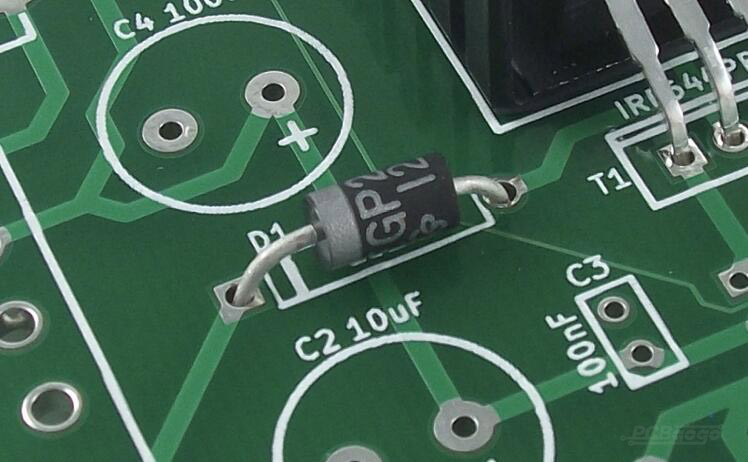
A silkscreen on PCB can provide the following information:
Polarity of parts;
Location of parts through reference designators;
Identify test points;
Identification numbers unique to each board;
Warning symbols.
2 Major PCB Silkscreen Methods
In the past few years, the primary method of PCB silkscreen has referred to using a stencil to directly apply ink to the board surface. Nowadays, there are two most common silkscreen PCB printing techniques, such as liquid photo imaging (LPI) and direct legend printing (DLP).
Liquid photo imaging (LPI):
This method is used when the line widths are greater than 4 mil. Liquid Photo Imaging is quite similar to the process used for the application of solder mask. In this a liquid photo-imageable epoxy is coated on to the laminate and then exposed with UV light. After this the board is developed and cured. It is much more accurate than manual screening.
Direct legend printing (DLP):
DLP is the most accurate of all these processes, but it is more expensive. In this process, an inkjet projector is used with acrylic ink that is applied onto the raw PCB directly from the CAD data. The ink is cured with UV light as it is printed. It should be noted, though, that the acrylic ink does not cure on boards with silver finishes.
The application of PCB silkscreen is done during PCB fabrication, but it’s used for the PCB assembly process steps, which mainly refer to placing or mounting components. There are some silkscreen markings used to place components accurately as follows:
Reference indicators - these identify the component types from the BOM.
Pin 1 indicator - this indicates which pins connect to what pads of the footprint.
Component outline – this, in conjunction with the landing pattern, indicates where the component should be placed.
Polarity indicators – these provide the orientation of polarized components.
For components with small numbers of pads or simple shapes, it may be acceptable for general placement to have the absence of the component outline. However, there still exists the possibility of asymmetrical placement, which may lead to problems during soldering, for example, tombstoning. The absence of reference, pin 1, and polarity indicators may lead to incorrect component orientation or placement, which could have a negative effect on device functionality.
Your silkscreen on your PCB in PCBGOGO
With over 10 years as an industry leader, PCBGOGO is one of the most experienced PCB and PCB assembly manufacturers in China. highly specialized not only in quick-turn PCB prototype and PCB assembly, but also in medium and small volume PCB fabrication. We can provide silkscreen on your PCBs, and we will do our best to meet your silkscreen requirements.
If you have any questions, please feel free to contact us at service@pcbgogo.com. We are happy to help you.

