PCBgogo

Electronic Project Engineer's Best Partner!
SMT Ordering Necessary Files & Info: Accurate information supports efficient quote & manufacturing processes
2998 3 Jul 05.2019, 15:20:36

1.For BOM

Please fill in designators(references), quantity, package and part numbers. For resistors or capacitors, if there is no part number, then value and package information is needed. It’s also better list components as PTH or SMD. Check our example BOM for reference.


2.For assembly orders

Please add polarity cathode or anode mark and pin 1 in silkscreen layer. 
If you do not want this information to be printed on the board, please send an individual assembly drawing file including those information to us. For cathode or anode, check the picture for reference, if use one line or one dot, we may get confused since sometimes it can be either cathode or anode. For pin 1, it’s ok to use dot.
It will be great if you have 3D images including into the Gerber file or send to us. 
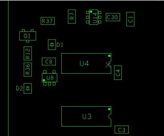

image.png


3.Pick&place/centroid file

We need completed pick&place file/centroid file including all the designators/references same as the ones in BOM, THT designators can be excluded. And designators in pick&place file should match the designators in silkscreen layer or assembly drawing file.


Prev: What Is Plated Half Hole PCB (Castellated Hole)?
Next:An Introduction to Rogers Material PCB by PCBGOGO
  • Comments(3)
Upload a photo:You can only upload 1 files in total. Each file cannot exceed 2MB.Supports JPG, JPEG, GIF, PNG, BMP
Browse
Submit
header
**

Mar 14.2024, 15:36:20

These are the standard file format used to convey PCB design data to PCB manufacturers. Strands NYT Gerber files include information about copper layers, solder mask, silkscreen, and drill files.

Reply

Submit
header
**

Dec 18.2023, 17:42:50

Specify PTH (Plated Through-Hole) or BuildNow GG SMD (Surface Mount Device) for components.

Reply

Submit
header
c****lyl

Nov 29.2023, 16:56:48

Clearly indicate the polarity, mark cathode or anode, and identify Pin 1 on the silkscreen layer of the PCB. If this information shouldn't be printed among us on the board, provide an individual assembly drawing file containing the necessary details.

Reply

Submit