PCB Vias -Something You Need To Know
PCB Vias -Something You Need To Know
As you know, PCB is a multi-layer construction with different links and passages between two or more adjacent layers. And PCB vias are extremely important for multi-layer PCB because it’s difficult and complicated to design and implement a multilayer board. So make it impossible to create the multilayer board with high quality and reliability without vias.
PCB vias are mainly in providing a conductive path for transferring an electrical signal from one PCB layer to another with the plated hole wall. But there are different types of vias and various options for the final appearance of the vias on the PCB surface. Even if all vias basically have the same function, it needs to define accurately each PCB types so that the subsequent PCB process will function well.
What is PCB via?
Via is one of the most important components as designing a multi-layer PCB. In fact, PCB via is drilling to be a hole on the circuit board, which is used for pads, electrically and thermally join traces, as well as polygons on various PCB layers. What’s more, it plays a role in creating a connection between various layers of a multi-layer PCB.
Three types of PCB via

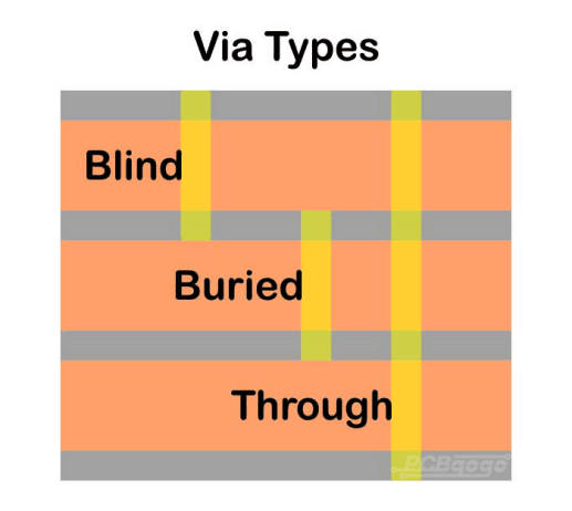
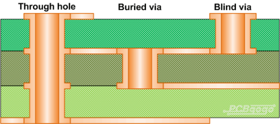
There are different types of PCB vias according to their functionality, however, the three most commonly used via are blind via, buried via as well as through hole.
Plated through hole (PTH)
Plated through hole is the most common type of via, in fact, it is a hole dug completely through the multiple layers of a PCB. As well as it’s the simplest type of via and is extremely cost-effective. But, it will take up more space on your PCB leaving you with a little space for your components.
Blind via
It’s difficult for a blind via to drill because it connects the exterior a majority of circuit with the inner layer present right below it. And you need to pay more attention to the depth of the hole as creating a blind via.
Buried via

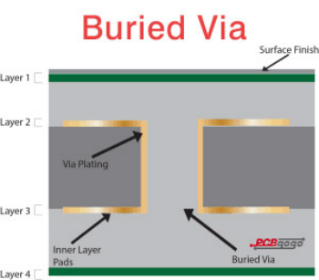
Buried Via is a copper plated hole that connects two or more internal layers of the board and is not accessible by the external layers. And it’s not possible to discover a buried vias in a PCB because it is "buried" under the external layer surfaces of the board. What’s more, buried vias also need an individual drill file. In general, buried via is used for high density interconnect (HDI) PCBs.
Why do you require the vias when designing a PCB?
There will not require the vias if the circuit is very simple. But it does required the vias when designing a multi-layer PCB.
1. In case of a multi-layer board, there have a decent density of components in vias.
2. With the multi-layer PCB increases, there will be more and more the density of traces. Traces can be run over and under each other in opposite directions over different layers. And vias can make the different traces present on different layers of a PCB to connect with each other. As well as vias play a role in acting as the vertical connection elements.
3. It’s easy to get into trouble in the routing process if you don’t use vias, and there will be placed densely ranging from BGA, connectors to even the components in a multi-layer PCB.
4. Vias allow the power and signals to travel between layers. And everything needs to be routed on a single plane and presence of surface mounted components if vias are not used, what’s more, make it difficult to do that in a multi-layer PCB.

Your PCB fabrication with vias in PCBGOGO
With over 10 years as an industry leader, PCBGOGO is one of the most experienced PCB and PCB assembly manufacturer in China. Highly specialized not only in quick-turn PCB prototype and PCB assembly, but also medium and small volume PCB fabrication. And we will try our best to fabricate your HDI PCB with buried vias or blind vias, as well as PCB with plated through hole, which will meet your demands with high quality, and make it cost-effective to reduce the PCB layers or size.
If you have any questions, please feel free to contact us with service@pcbgogo.com, we will be happy to help you.

