
 日本語
日本語
 한국어
한국어

What Is GND in Electronics and PCB Grounding Guide
GND in electronics is the node used as the circuit voltage reference and, in most designs, part of the current return path. It is often labeled 0 V, but it is not automatically the negative battery terminal, protective earth, or chassis. PCB grounding works only when return current paths and connection points are deliberately controlled.
Why the Ground Symbol Causes So Much Confusion
GND in electronics identifies a reference node, but the same ground symbol can represent different physical connections in different systems. A schematic label alone does not prove that two nodes share the same conductor, earth bond, noise environment, or safety role.
Voltage is always measured as a difference between two points. A 3.3 V signal normally means the signal is 3.3 V above its local GND node. Current also requires a complete loop, so its return path through traces, planes, cables, capacitors, and supplies affects the voltage at every point in that path.
For reliable PCB grounding, trace the complete current path from source to load and back. This is more useful than simply counting ground symbols, because copper has both resistance and inductance—effects that become increasingly important at higher frequencies.
What GND Means in a Circuit
GND is the designated zero volt reference used to describe other node voltages in a circuit. It provides a common measurement point and often carries return current, but it may float above or below earth potential.
A battery powered device can operate with no physical connection to earth. Its negative terminal may be selected as GND, which makes all other voltages positive relative to that node. In a split supply, the midpoint can be GND, with one rail at positive voltage and another at negative voltage.
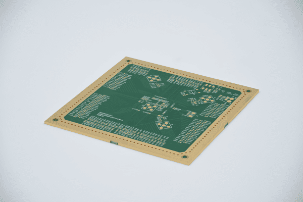
Is GND the Same as the Negative Terminal
GND is the same as the negative terminal only when the circuit intentionally connects those nodes and chooses that point as the reference. The labels describe different ideas: negative identifies polarity relative to another point, while GND identifies the chosen reference or return network.
A current sense resistor may sit between battery negative and system ground. Joining those nodes elsewhere bypasses the measurement. Reverse polarity protection can also place a switch between the connector negative and the local return. Isolated converters create secondary grounds with no direct conductive connection to the primary side.
Common Ground Types Compared
Ground types are names for electrical roles, and one physical node may serve several roles when the system architecture allows it. The labels help designers decide where currents should flow and where connections must remain controlled.
This table compares common ground labels and the question each one answers.
| Ground type | Primary role | Typical connection question |
|---|---|---|
| Signal ground | Reference for logic or measured signals | Which return path stays with the signal |
| Power ground | Return for converters, motors, and high current loads | Where large current creates voltage drop |
| Analog ground | Reference for low level analog circuits | How digital or switching current is kept away |
| Digital ground | Return for logic and clock currents | How fast edge current reaches its source |
| Chassis ground | Connection to enclosure or structural metal | Where shields and fault current meet the enclosure |
| Protective earth | Safety bond to the installation earth system | How hazardous fault current clears protection |
Names do not create isolation. Two nets remain separate only if the schematic, PCB, components, connectors, and mounting hardware preserve that separation.
Why PCB Return Paths Matter
PCB return paths matter because every signal current forms a loop, and loop impedance affects voltage error, crosstalk, and radiated emissions. At low frequencies, return current spreads according to resistance. At higher frequencies, it concentrates near the signal path where loop inductance is lowest.
A continuous ground plane beneath a trace gives return current a short, adjacent path. Cutting the plane or routing across a split forces current around the opening, increasing loop area and coupling noise into other circuits. Plane gaps can also create slot-antenna behavior.
Layer transitions need the same attention. When a signal changes reference layers, place a nearby ground stitching via or suitable return component so the return current can transition with it. Without one, the current must search for a distant connection, making the effective loop much larger.
PCB Grounding Practices That Reduce Noise
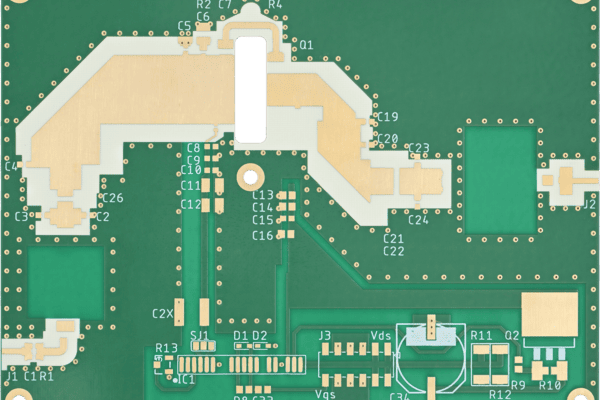
Good PCB grounding creates a low impedance reference while controlling where high current and fast edge returns travel. A solid plane helps, but placement and routing determine whether sensitive and noisy currents share the same local path.
Use a continuous reference plane: Dedicate a layer when possible and avoid slots under high speed or sensitive traces.
Partition by function: Place analog acquisition, digital processing, power conversion, and connectors so their current loops remain physically clear.
Keep switching loops compact: Place the input capacitor, switch, diode or synchronous device, and return connection close together in a converter.
Decouple at the IC: Connect each bypass capacitor with a short path between the power pin and ground reference. Long traces add inductance and reduce high frequency effectiveness.
For many systems with one mixed-signal converter and low digital current, a solid single ground plane is often effective. More complex systems may require a different architecture. Follow the specific IC datasheet and the actual system current paths instead of splitting ground by habit.
Once the grounding architecture is defined, PCBgogo can fabricate multilayer PCBs from the released stackup and provide electrical testing. Put plane assignments, controlled impedance, copper weight, and any isolation requirement in the manufacturing data so the built board preserves the intended reference structure.
PCBgogo - Reliable, High-Quality PCB Manufacturing
Save time and money with an all-in-one solution for PCB fabrication, assembly, and parts. Reduce vendor coordination, avoid split shipments, and get consistent, reliable quality.
Get Free Quote >
Grounding Standards and Safety Boundaries
Grounding standards form a stack that separates signal integrity, electromagnetic compatibility, and protective safety functions. A quiet signal ground is not automatically a compliant protective earth connection.
IPC 2221: Provides generic printed board design guidance used when planning conductors, spacing, and board structures.
IEC 61000 series: Covers electromagnetic compatibility test methods and limits that can expose weak grounding, shielding, or filtering.
IEC 60664: Addresses insulation coordination and inputs used to determine creepage and clearance for low voltage equipment.
Product safety standard: The equipment category determines protective earth, accessible voltage, insulation, leakage, and fault requirements.
Compliance testing evaluates the finished product in its enclosure with cables and intended power. A PCB layout is one part of that evidence, not a substitute for product level review.
Common PCB Grounding Mistakes
Common PCB grounding mistakes interrupt return paths or allow high current to modulate a sensitive reference. The resulting board may pass a simple continuity test while failing under load, at temperature, or during EMC testing.
Routing across a split: The signal crosses a plane gap but its return current cannot, which increases loop area and noise.
Sharing a narrow return: A motor, LED, or converter current flows through the same thin trace used as a sensor reference.
Remote decoupling: The capacitor is electrically connected but too far from the IC pins to control fast current demand.
Accidental chassis bonds: Mounting screws, connector shells, shields, and test equipment join grounds at unplanned locations.
Review the board by drawing each important current loop. That exercise usually finds the mistake faster than inspecting copper area alone.
Frequently Asked Questions About GND
These questions clarify how the GND label relates to voltage, negative terminals, earth, planes, and mixed signal design.
Does GND always equal 0 V?
GND is defined as 0 V within its local reference system. It can still sit above or below earth potential or another isolated circuit ground.
Can a circuit work without earth ground?
Yes. Battery powered and isolated circuits commonly operate without an earth connection. They still need a complete local current loop and a defined voltage reference.
Should analog and digital ground planes be split?
Not automatically. Many mixed signal designs work better with one continuous plane and careful placement, while some systems need a controlled split or star connection. Follow the device datasheet and return current analysis.
Why is a ground plane better than a thin trace?
A plane generally provides lower resistance and inductance plus a nearby return path for signals. It also reduces shared impedance when currents are placed and routed correctly.
Conclusion
GND in electronics is a reference and return network whose real behavior depends on current flow and impedance. Name each ground by its role, preserve continuous return paths, and define every connection among signal ground, power ground, chassis, and protective earth before layout release.





