
 日本語
日本語
 한국어
한국어

Integrated Circuits Types Packages and PCB Assembly Guide
Integrated circuits combine transistors and other electronic elements on a semiconductor die, then connect that die to a PCB through a protective package. Designers must choose the electrical function and package together because pin count, pitch, exposed pads, heat flow, inspection access, footprint accuracy, and component handling all affect PCB layout and assembly yield.
Why the IC Package Matters as Much as the Function
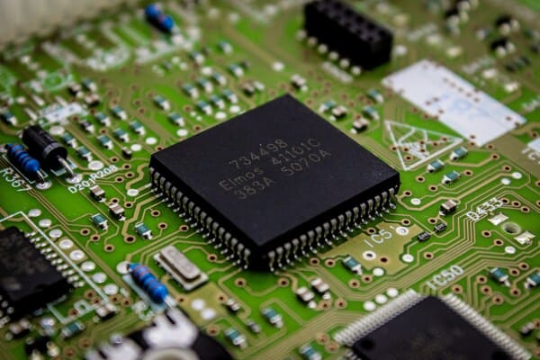
Integrated circuits perform electronic functions on a semiconductor die, while the package protects the die and connects it to the PCB. The same circuit function may be sold in several packages, and each package affects board area, routing, thermal performance, inspection, and rework.
An integrated circuit combines many transistors into a small circuit on a semiconductor chip. It is useful to distinguish among the wafer, the die, and the packaged chip: a wafer is the semiconductor material used during fabrication, a die is an individual circuit cut from that wafer, and the package is the protective enclosure and electrical interface around the die. This distinction helps prevent ambiguity when a BOM refers to the complete component as an IC while a failure report identifies an issue within the die.
How Integrated Circuits Work
Integrated circuits work by arranging semiconductor devices and metal interconnects to implement a defined analog, digital, power, or mixed-signal function. Transistors act as switches or controlled-current devices, while on-chip resistors, capacitors, diodes, memory cells, and interconnects complete the circuit.
The die is fabricated through repeated deposition, patterning, etching, doping, and metallization steps on a wafer. After electrical wafer testing, usable dies are separated, attached to a lead frame or substrate, connected by wire bonds or bumps, enclosed in a package, and tested again.
Modern semiconductor wafers are commonly 300 mm in diameter and approximately 0.775 mm thick. Many identical integrated circuits are formed on one wafer, then diced and packaged into components designed to withstand handling and connect reliably to a larger circuit board.
Common Types of Integrated Circuits
Integrated circuit types are grouped by the signals they process and the job they perform. Many devices combine categories, but the grouping helps identify the most important layout and test risks.
Operational amplifier: This analog IC amplifies a voltage difference and appears in filters, sensor front ends, and control loops. Input offset, noise, bandwidth, and supply range guide selection.
Logic and memory: Digital ICs interpret defined logic levels and store or transform data. Edge rate, timing, decoupling, and interface voltage dominate the PCB design.
Microcontroller: A microcontroller combines a processor, memory, timers, and communication peripherals. It needs defined reset, clock, programming, power, and firmware configuration.
Analog to digital converter: A mixed signal ADC samples an analog input and produces a digital code. Reference voltage, grounding, input settling, and clock noise directly affect measurement quality.
The application category guides the layout, but the device datasheet remains the authority. Two ICs with the same function can require different decoupling, thermal, or grounding arrangements.
Integrated Circuit Package Types Compared
Integrated circuit packages differ in mounting method, lead access, connection density, thermal path, and inspection method. Package names describe a family, while the manufacturer drawing defines the exact dimensions and tolerances.
This table compares package families commonly encountered in PCB design and assembly.
| Package | Connection style | Main advantage | Assembly concern |
|---|---|---|---|
| DIP | Through hole leads on two sides | Easy socketing and manual handling | Large board area and drilled holes |
| SOIC | Gull wing leads on two sides | Visible joints and familiar SMT process | Lead pitch and coplanarity |
| QFP | Gull wing leads on four sides | High visible pin count | Fine pitch bridging and lead damage |
| QFN | Pads and thermal pad under body | Compact size and short electrical path | Hidden joints and paste balance |
| BGA | Solder ball array under body | High connection density and efficient escape | X ray, warpage, and via strategy |
Common IC package families include DIP, QFP, BGA, SOIC, and TSOP. Their connections may appear as leads on two sides, leads on four sides, or contact pads underneath the package.
The package abbreviation is only a starting point: body dimensions, pin count, lead pitch, thermal characteristics, and land-pattern requirements can vary substantially within a single family. Always verify the specific component datasheet before finalizing the PCB footprint.
How to Build the Correct IC Footprint
A correct IC footprint converts the package drawing into solderable PCB lands, mask openings, paste apertures, courtyard, polarity marks, and assembly data. Reusing a footprint based only on pin count or package name can place every pin in the right order but the pads in the wrong location.
Use the manufacturer drawing: Confirm body dimensions, terminal width, pitch, datum, tolerances, pin one, and the recommended land pattern for the exact orderable package.
Check exposed pads: Determine copper size, mask definition, paste coverage, thermal vias, and whether vias under paste must be filled or capped.
Match symbol and pin map: Verify every schematic pin against the datasheet, including no connect, exposed pad, duplicated power, and alternate function pins.
Verify rotation data: The PCB footprint, centroid file, assembly drawing, and machine library must agree on pin one and zero degree orientation.
In PCB documentation, a package footprint describes the component’s physical interface, while the PCB land pattern defines the solderable pad geometry. Keeping those definitions clear helps designers, assemblers, and library owners exchange accurate component data.
Assembly Challenges for Fine Pitch QFN and BGA Devices
IC assembly challenges increase when joints become smaller, move beneath the package, or carry significant heat. Paste printing, placement, board flatness, reflow, moisture control, and inspection must work as one process.
Fine pitch QFP leads: Excess paste, placement offset, or lead deformation can create bridges. Insufficient paste or poor wetting can leave an open heel joint.
QFN thermal pads: Too much center paste can float the package and starve perimeter joints. Too little can reduce thermal and mechanical performance.
BGA solder arrays: Joints are hidden from normal optical inspection. X ray can reveal bridges, missing balls, and void patterns, while functional or boundary scan testing checks electrical behavior.
Moisture sensitive packages: Absorbed moisture can expand rapidly during reflow and damage the package. J STD 020 classifies sensitivity, while J STD 033 defines handling and floor life controls.
BGA and LGA mounting recommendations must be validated for the specific product and assembly process, particularly in high-power or high-voltage applications. Generic package guidance is a starting point, not proof of assembly readiness.
For builds that combine SMD, through hole, QFN, or BGA parts, PCBgogo publishes mixed assembly, AOI, functional test, and DFM support. Provide the exact package drawings and special inspection requirements so the assembly plan reflects the real component set.
PCBgogo - Reliable, High-Quality PCB Manufacturing
Save time and money with an all-in-one solution for PCB fabrication, assembly, and parts. Reduce vendor coordination, avoid split shipments, and get consistent, reliable quality.
Get Free Quote >
Standards and Data Needed for IC Assembly
IC assembly standards form a stack covering land patterns, soldering processes, moisture handling, and finished assembly acceptance. The BOM and drawings still need to identify the exact device and customer requirements.
IPC 7352: Provides guidance for surface mount land pattern design and supersedes earlier general land pattern references.
IPC 7525: Addresses stencil design guidelines used to control solder paste deposition.
J STD 020: Classifies nonhermetic surface mount devices for moisture and reflow sensitivity.
J STD 033: Defines handling, packing, shipping, and use controls for moisture sensitive devices.
J STD 001 and IPC A 610: Pair soldered assembly process requirements with postassembly acceptability criteria.
A standard does not resolve a BOM that omits the package code or a centroid file with incorrect rotation. Include manufacturer part number, package, reference designators, approved alternates, polarity drawing, placement data, programming instructions, and test requirements in the release.
Frequently Asked Questions About Integrated Circuits
These questions connect basic IC terminology with the decisions that affect PCB design and assembly.
What is the difference between an IC and a chip?
An integrated circuit is the electronic circuit formed on the semiconductor die. Chip can mean the die or the packaged component, so manufacturing documents should use die, package, and component precisely.
Which IC package is easiest to solder by hand?
DIP and larger pitch SOIC packages are usually the most accessible for hand soldering. Fine pitch QFP, QFN, and BGA packages need tighter process control and often automated equipment.
Why do QFN packages have an exposed center pad?
The exposed pad commonly improves heat transfer and can provide an electrical ground connection. Its copper, paste, and via design must follow the exact device datasheet.
How are BGA solder joints inspected?
X ray inspection is commonly used because the joints are hidden beneath the package. Electrical, boundary scan, or functional testing adds evidence that the assembled device operates correctly.
Conclusion
Integrated circuits must be selected as electrical functions and physical packages at the same time. Verify the exact drawing, build a controlled footprint, design the thermal and routing path, and give the assembler clear handling and inspection requirements before releasing the PCB.





