
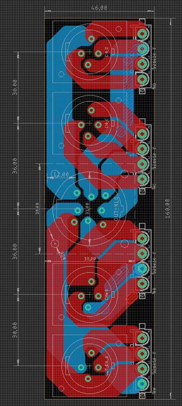
Big Old Fat Traces (High Current PCB)
I'm designing a PCB for an audio amplifier that has the potential to put out 40A (instantaneous), and honestly, I'm out of my comfort zone. The connectors are rated to a min 35A and I'm basically going for big fat traces to take the current load.
All components in the assembly are pass-thru connectors, nothing to overheat besides the board itself.
The narrowest neck is 5.5mm thick (besides certain spots where I have to taper down by the molex)
I plan on using 4oz copper
I read about doing a waves solder to help as well, same goes for buss bars
Trace/Pad clearances are 50mil (plz don't harass me for using mm and mil)
What I'm looking for answers to
1) Is this just dumb? Am I crazy?
2) Any suggestions
3) General high current PCB design suggestions
Proto-types for testing will be done, but I'd rather not spend the money if this won't work out of the box.
Thanks for the feedback


- Comments(1)
A****min
Jun 19.2019, 09:32:45
even though your board may be 4 oz copper : the plating in the holes won't be ! So whenever you experience a layer-hop : shoot a ring of via's around the holes.
For example : your power arrives on bottom layer to a capacitor pin , then leaves on top layer. Don't bank on the solder and the pin ! it may not flow up far enough in the hole to guarantee a nice solder fillet under the component. It wouldn't be the first board where the plating burns out...

