




 日本語
日本語
 한국어
한국어

Wireless Charger Module Fast Charging Board PCB Design Guide
A wireless charger module fast charging board PCB works only as well as the system around it. The controller, copper, coil, shielding, enclosure and power adapter all affect charging speed and temperature. If you are selecting a module for a product or designing your own transmitter board, start with the phone or receiver you need to support, then design backward from its power profile and mechanical position. This guide explains the decisions that matter most, the PCB details that commonly limit performance, and a practical way to validate a prototype before production.
What a Fast Charging Wireless Module Actually Includes
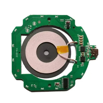
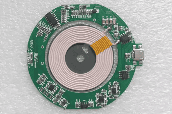
In most products, the transmitter is a small PCB assembly with a power input, a controller, switching devices, a resonant network and a transmit coil. Ferrite or another specified magnetic shield directs flux toward the receiver and reduces interaction with nearby metal. Temperature sensing, current measurement and firmware support power control and foreign object detection, or FOD. The receiver has its own coil, rectifier and charging circuitry; the transmitter does not directly determine the battery charging current.
A board advertised as "15 W" or "25 W" describes a potential operating class, not a guarantee that every phone will charge at that rate. The adapter must supply sufficient power, the receiver must negotiate the relevant profile, alignment must be good, and the thermal conditions must allow sustained operation. Treat the PCB, coil, magnetic materials and enclosure as one design rather than interchangeable parts.
Choose the Charging Profile Before Laying Out the PCB
The first purchasing question is compatibility. The Wireless Power Consortium’s Qi family includes older Basic Power Profile products, 15 W Extended Power Profile designs, Qi2 magnetic designs at 15 W, and Qi2 25W. A proprietary “fast charge” claim is different from a certified Qi power profile. Confirm the intended receiver models and the exact transmitter controller or reference design before committing to a layout.
| Design target | Typical power class | Key design check |
|---|---|---|
| Qi basic | Up to 5 W | Broad compatibility and stable positioning |
| Qi EPP | Up to 15 W | Receiver support, authentication and thermal headroom |
| Qi2 magnetic | Up to 15 W | Magnet alignment and complete mechanical stack |
| Qi2 25W | Up to 25 W | Supported ecosystem, adapter, loss and FOD calibration |
For a desk accessory used with mixed older devices, an established 15 W design may fit. For a product built around magnetic alignment, evaluate a Qi2 design. If 25 W is a product requirement, verify the complete Qi2 25W design path, including the selected receiver ecosystem, adapter, magnetic stack and certification plan. Higher rated power increases the importance of copper loss, FOD calibration and enclosure temperature.
PCB Design Decisions That Influence Real Charging Speed
Keep the High Current Loop Short
The power path from the input connector through the switching stage and resonant components to the coil carries pulsed current. Short, wide copper paths and a compact loop reduce resistive loss and unwanted emissions. Use the controller manufacturer’s reference layout as the starting point. If current must change layers, use enough vias for the expected current and check the temperature rise in the actual board stack. Do not place a thin neck between a wide plane and a high current pad.
Place local decoupling close to the switching devices and their return path. Keep quiet sensing and communication traces away from noisy power nodes. For current sense resistors, route the measurement traces directly from the sense pads as a Kelvin connection so copper voltage drop does not become a false current reading. This matters because inaccurate loss measurement can make FOD unreliable.
Design the Coil and Mechanical Stack Together
The coil’s inductance, resistance, diameter and position must match the controller design and supported profile. Its distance to the receiving coil includes the charger cover, adhesive, air gap and the receiver’s own enclosure. Even a small mechanical change can reduce coupling, raise heat or change the FOD result. Document the coil part number, ferrite geometry, adhesive thickness and final top surface height in the manufacturing package.
Avoid placing unplanned metal hardware in the active magnetic field. Screws, decorative rings and nearby copper can absorb energy and heat. A magnetic alignment design also needs the specified magnet arrangement and polarity. A planar PCB coil can suit an especially thin custom product, but its losses and behavior must be measured in the finished stack; it should not be assumed equivalent to a wound coil.
Give Heat a Deliberate Escape Path
Losses appear in the adapter input path, switching devices, resonant capacitors, coil and nearby conductive materials. Provide enough copper area and thermal vias where the component data sheet calls for them, while preserving the controller’s layout and magnetic keepouts. Keep temperature sensors thermally coupled to the locations the control algorithm expects. A comfortable open-bench board can become hot under a plastic cover or inside a car dashboard.
Test at the highest expected ambient temperature and with the real enclosure. Record charging power over time, not just the first minute. A board that reaches a high peak and immediately throttles may deliver a worse user experience than a cooler design with a lower but steady output.
FOD and Certification Need Final Assembly Testing
Foreign object detection estimates whether power is being lost into an unintended object, such as a coin or key. It depends on accurate electrical measurement and calibration with the final coil, shielding, enclosure and firmware. Changing the coil, cover thickness or nearby metal after calibration can invalidate the result. Include representative misplaced devices and specified foreign objects in the validation plan; do not disable protective functions to make a prototype appear faster.
Qi certification belongs to a tested product or eligible complete subsystem, not to a loose coil or controller IC. A transmitter module that uses a certified component is not automatically Qi Certified. If the product will carry a Qi or Qi2 logo, check the Wireless Power Consortium requirements for the exact profile and the finished configuration. An embedded certified transmitter subsystem may simplify the route, but its installation conditions, including surface distance and surrounding materials, still matter.
A Practical Prototype and Test Plan
Before ordering boards, build a concise design package: schematic, Gerber files, stackup, bill of materials, placement data, coil and ferrite specifications, firmware version and the intended test conditions. Ask the PCB manufacturer to review copper widths, via structures, material selection, solder mask clearances and any unusual thermal or mechanical requirements. For assembly, specify polarity, programming, inspection and the functional tests you expect rather than assuming a visual check covers charging performance.
| Test | What to record | Why it matters |
|---|---|---|
| Input and negotiation | Adapter voltage, current and active profile | Separates input limits from charger limits |
| Alignment and gap | Center and offset positions with final cover | Exposes coupling and usability issues |
| Sustained load | Power and temperatures over time | Reveals thermal throttling |
| Foreign objects | Specified objects, fault response and recovery | Checks protective behavior |
| Receiver mix | Target models and charge behavior | Checks practical compatibility |
Run this matrix with the intended adapter and several target receivers. Repeat the key cases after assembly changes or a new PCB revision. Capture input voltage and current, negotiated profile where observable, receiver charging behavior, component and cover temperatures, fault codes and test duration. Compare results against written acceptance limits set for your product. These records make a manufacturing issue easier to distinguish from an electrical or mechanical design issue.
Common Problems and What to Inspect First
The Phone Charges Slowly Despite a High Rated Board
Check the receiver’s supported profile and the adapter’s output first. Then verify coil alignment, cover thickness and the negotiated operating mode. Compare cold and warm performance. If speed falls only after several minutes, inspect thermal throttling before changing the resonant network.
Charging Repeatedly Starts and Stops
Look for input voltage sag, unstable connectors, incorrect coil or capacitor values, communication problems and FOD trips. Keep a scope capture of the input rail and a log of controller fault states. A board that works without the enclosure but fails when assembled points strongly toward magnetic or mechanical interaction.
The Charger or a Nearby Object Becomes Too Hot
Stop the test and locate the heat source. Measure the coil, switching stage, connector and any metal near the field. Check for alignment errors and missing or incorrect shielding. Avoid treating a larger copper pour as the only fix: it will not correct poor coupling, a bad magnetic stack or inaccurate FOD calibration.
How PCBgogo Can Support the Build
Once the electrical and mechanical requirements are defined, PCBgogo can review the PCB stackup and manufacturability, fabricate prototype boards and assemble the PCBA. Its published capabilities include engineering review for materials and copper features, SMT assembly, inspection methods such as AOI and X-ray where applicable, and customer-defined functional testing. For a wireless charging project, provide the complete stack and a specific test procedure so the quote and build reflect the real product. PCB fabrication and assembly support repeatability; performance validation and any Qi certification remain part of the product development plan.
PCBgogo - Reliable, High-Quality PCB Manufacturing
Save time and money with an all-in-one solution for PCB fabrication, assembly, and parts. Reduce vendor coordination, avoid split shipments, and get consistent, reliable quality.
Get Free Quote >
Frequently Asked Questions
Can I Replace a 15 W Module With a 25 W Board?
Not safely as a simple drop-in change. Confirm the adapter, receiver profile, coil, shielding, enclosure, thermal design and certification scope. Recheck the PCB current path and rerun functional and FOD testing.
Is a Two-Layer PCB Enough for a Wireless Charger?
It can be for some reference designs, but layer count alone does not establish performance. Current return paths, copper weight, heat spreading, grounding and noise control matter more. Follow the selected controller design guidance and verify temperature and emissions on the finished assembly.
Does a Controller IC Make the Whole Charger Qi Certified?
No. An individual controller IC cannot be Qi Certified. Certification applies to a tested complete transmitter or eligible subsystem under its defined conditions. The final product needs the appropriate assessment for its configuration and intended branding.
Build for Sustained Performance
A successful wireless charger module fast charging board PCB is a validated system, not a power number printed on a product page. Select the correct profile, preserve the reference design’s electrical details, control the magnetic and mechanical stack, and test power, heat and FOD in the final enclosure. When those inputs are ready, send PCBgogo the PCB and assembly files together with your stackup and acceptance criteria to move from a promising prototype toward a repeatable build.





