
 日本語
日本語
 한국어
한국어

Memory PCB Explained: Types, Design & Manufacturing
KEY DEFINITION A memory PCB is a printed circuit board built to host memory chips such as RAM, ROM, or flash and route high-speed signals between those chips and a processor. A RAM PCB is the volatile-memory subtype used for temporary data storage, and it typically needs tighter impedance control and more layers than a standard memory board.
Every time a laptop boots or a phone unlocks in under a second, a memory PCB is quietly doing the heavy lifting behind the scenes.
This guide covers what memory PCBs are, how a RAM PCB fits into that broader category, and the design and manufacturing factors that separate a reliable board from a flaky one.
Where Memory PCBs Show Up
The right memory PCB for a project depends on how fast data needs to move and how much room there is to route it.
Laptop and desktop RAM modules: SO-DIMM and UDIMM boards carry DDR4 or DDR5 chips and rely on tight length matching between traces so every bit in a data burst arrives at the same time.
Graphics cards: GDDR memory PCBs sit close to the GPU package and use short, wide traces to support the bandwidth modern rendering workloads demand.
Servers and data centers: RDIMM and LRDIMM boards add buffering circuitry to the memory PCB so a single system can address hundreds of gigabytes without signal degradation.
Automotive control units: EEPROM-based memory PCBs store calibration data and firmware in engine and body control modules, where vibration resistance matters as much as speed.
Smart cards and payment terminals: Compact memory PCBs hold EEPROM or flash chips that retain account data without power, a requirement no volatile RAM PCB can meet.
Each of these use cases points to a different memory type, which is where the real design decisions begin.
Memory PCB vs. RAM PCB: How the Types Break Down
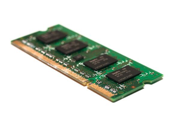
A memory PCB is any circuit board engineered to carry integrated circuits that store data, whether that storage is temporary or permanent. The category splits into two branches: volatile memory, which loses its contents without continuous power, and non-volatile memory, which retains data indefinitely.
A RAM PCB is the volatile branch of the memory PCB family, built to hold DRAM or SRAM chips that a processor reads and writes constantly during operation. Because a RAM PCB handles continuous high-frequency traffic, it typically needs tighter trace impedance tolerances and more layers than a board built for occasional, low-speed access, such as an EEPROM board.
Non-volatile memory PCBs cover EEPROM, NAND flash, and NOR flash boards, and each type suits a different balance of speed, capacity, and data retention. EEPROM boards handle small-capacity data that gets rewritten byte by byte, NAND flash boards pack high density into drives like SSDs and USB sticks, and NOR flash boards trade some density for byte-level addressing that suits BIOS and firmware storage.
The table below compares typical layer counts and applications across common memory PCB types.
| Memory Type | Volatility | Typical Layer Count | Common Application |
|---|---|---|---|
| SRAM PCB | Volatile | 4 to 6 layers | CPU cache, real-time control systems |
| DRAM / RAM PCB (DIMM) | Volatile | 6 to 10 layers | Laptop, desktop, and server main memory |
| NAND Flash PCB | Non-volatile | 4 to 8 layers | SSDs, USB drives, memory cards |
| EEPROM PCB | Non-volatile | 2 to 4 layers | Automotive ECUs, smart cards |
What Actually Drives Memory PCB Design Decisions
What actually determines whether a memory PCB performs reliably comes down to a handful of layout and manufacturing choices made before the first board is fabricated.
Layer stack-up: More layers create dedicated power and ground planes that isolate high-speed signal layers from noise, which is why DIMM and GDDR boards rarely ship as simple 2-layer designs.
Controlled impedance: DDR4 and DDR5 interfaces run single-ended and differential signals that must stay within a tight impedance window, or the board risks reflection and data corruption at speed.
Trace length matching: Every bit in a data byte needs to reach the memory controller within a fraction of a nanosecond of the others, so trace lengths across a memory PCB are matched closely.
Via and BGA fanout: Modern DRAM and flash packages ship in fine-pitch BGA footprints, and routing signals out from under a dense ball grid without violating spacing rules takes precise fabrication tolerances.
Material selection: FR-4 covers most consumer memory PCBs, but higher-speed server and networking modules often move to low-loss laminates to control signal attenuation at gigahertz frequencies.
Getting these factors right on paper is only half the job. The board still has to be fabricated to those exact tolerances, which is where the manufacturing partner matters.
Why Choose PCBgogo for Memory PCB Manufacturing?
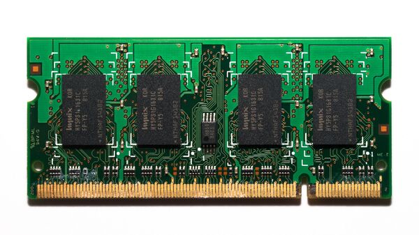
High-speed memory boards require more than dense routing. They need a manufacturer that can consistently build fine traces, complex stack-ups, controlled-impedance lines, and reliable BGA fan-outs.
High-density multilayer construction
Build memory PCBs from 1 to 40 layers, supporting applications ranging from EEPROM modules and SSD controller boards to complex server memory designs.Fine-line routing for dense layouts
Trace and spacing capabilities reach 2/2 mil on inner layers and 2.5/2.5 mil on outer layers, helping designers route high-density memory buses within limited board space.HDI and fine-pitch BGA support
PCBgogo supports 1–3-step HDI, 0.1 mm laser-drilled holes, and published BGA pitches down to 0.1 mm—providing greater routing flexibility beneath DRAM, NAND flash, and memory-controller packages.Controlled impedance with engineering confirmation
Submit your stack-up, target impedance, and tolerance requirements before production. PCBgogo’s engineers will confirm the specifications, while most controlled-impedance boards undergo testing to help verify the finished result.
Whether you are developing a DDR module, SSD, embedded storage device, or another high-density memory product, PCBgogo can support your project from prototype to batch production.
Upload your Gerber files and get a quote today—or contact PCBgogo to confirm your stack-up, HDI, and impedance requirements before ordering.
Quality Standards Memory PCBs Need to Meet
Certifications are not a single checkbox for memory PCBs. They are a stack of standards that each cover a different part of the board's reliability.
JEDEC standards: Define the electrical, mechanical, and pinout specifications for DRAM and DIMM modules, which is what lets a memory PCB built to spec interface correctly with a given chipset.
IPC-6012: Sets the qualification and performance requirements for rigid printed boards, covering plating thickness, hole quality, and other fabrication tolerances relevant to memory PCBs.
IPC-2221: Provides the generic standard for PCB design, including the conductor spacing and sizing rules that inform impedance-controlled memory layouts.
RoHS and REACH: Restrict hazardous substances such as lead, and most memory PCBs bound for consumer or EU markets need to comply regardless of memory type.
None of these standards alone guarantees a working board. Together, they cover the design rules, the fabrication process, and the material safety a memory PCB needs to pass qualification.
Challenges and Trends Shaping Memory PCB Design
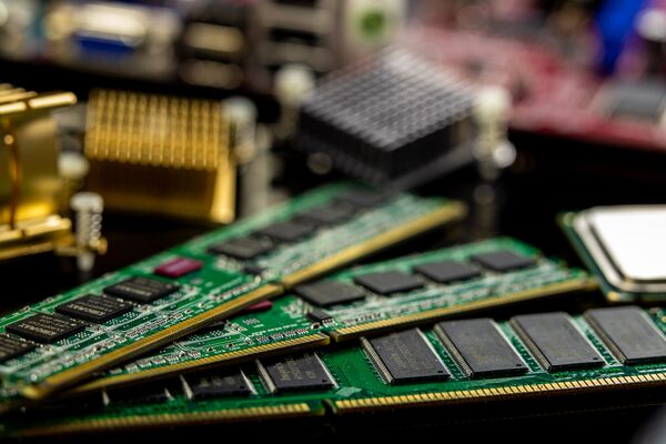
Memory PCBs face a familiar industry tension: every new generation demands more bandwidth from a board that keeps shrinking.
Signal integrity at higher speeds: DDR5 and LPDDR5 push data rates that leave less margin for impedance mismatch or crosstalk than earlier generations tolerated.
Miniaturization: Mobile and wearable devices are pushing memory PCBs toward smaller footprints, which shifts more designs toward HDI and fine-pitch BGA routing.
Thermal management: Dense DRAM and flash arrays generate heat in a small area, and a memory PCB's copper distribution has to help pull that heat away from the chips.
Cost versus performance: Low-loss laminates and tighter impedance tolerances improve signal integrity but add cost, so most designs balance material choice against the speed the application actually needs.
Standards migration: As DDR5 and LPDDR5 become mainstream, older memory PCB designs built around DDR4 tolerances are being redesigned rather than simply re-spun.
These pressures are pushing memory PCB design and RAM PCB design closer together as both chase the same signal integrity limits.
FAQ About Memory PCBs
What is the difference between a memory PCB and a RAM PCB?
A memory PCB is the broad category covering any board built to host data-storage chips, volatile or non-volatile. A RAM PCB is specifically the volatile subtype, designed to carry DRAM or SRAM chips that lose their contents without continuous power.
How many layers does a typical memory PCB have?
It depends on the memory type and speed. A basic EEPROM board might use as few as 2 layers, while a high-speed DDR5 DIMM commonly runs 8 layers or more to isolate signal traces with dedicated ground planes.
What surface finish works best for memory PCBs?
ENIG is the most common choice for memory PCBs because it offers a flat, solderable surface that suits the fine-pitch BGA packages memory chips typically use. HASL is sometimes acceptable for simpler, lower-density boards where cost matters more than pad flatness.
Can a memory PCB be repaired if it fails?
Surface-level issues like a cracked trace or a failed solder joint can sometimes be reworked, but a board with a delaminated internal layer or a failed via usually needs to be replaced. Because memory PCBs pack signals so densely, tracing an internal fault is rarely cost-effective compared to fabricating a new board.
Why do memory PCBs need controlled impedance?
High-speed memory interfaces like DDR4 and DDR5 send signals as fast pulses that reflect or distort if the trace impedance does not match the driver and receiver. Controlled impedance keeps that mismatch within a tolerance the signal can absorb without corrupting data.
Conclusion
A memory PCB's job looks simple on paper: hold data and move it fast. In practice, hitting that goal depends on layer count, impedance control, and fanout decisions made long before the board reaches fabrication, and a RAM PCB carries the strictest version of those requirements. Get the design factors right early and confirm they hold up in manufacturing, and the board will keep pace with whatever memory standard comes next.





