



 日本語
日本語
 한국어
한국어

What Is a Bluetooth Module? Custom Bluetooth PCB Module for Your Project
KEY DEFINITION A Bluetooth module combines a 2.4 GHz radio, controller, clocking, firmware, and often an antenna. A reliable Bluetooth circuit board requires the right radio architecture, the specified antenna keepout, a controlled 50 ohm RF path, and performance validation inside the final enclosure.
A wireless product can pass a bench test and still lose range after the battery, display, or enclosure is installed. That failure usually starts with a decision made before routing, such as the wrong antenna position, a noisy power rail, or a module selected without enough memory and interface capacity.
This guide follows the real development sequence from Bluetooth module selection through circuit design, PCB layout, manufacturing, testing, cost planning, and production support.
What Is a Bluetooth Module
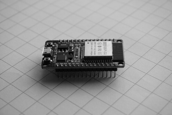
A Bluetooth module is a self-contained radio subsystem that places the Bluetooth controller, RF matching, clocks, and supporting components on one small PCB or package. Many modules also include an antenna, protocol stack, application processor, regulatory approvals, and a software development kit.
A module reduces RF design risk because its radio network is already characterized. The carrier PCB, nearby metal, power integrity, firmware, and enclosure can still change radiated performance.
Types of Bluetooth Modules
Bluetooth modules are best grouped by radio capability and by where the application software runs. The right category depends on audio requirements, power budget, host architecture, data throughput, and the product qualification path.
| Module type | Best fit | Power and data behavior | PCB integration note |
|---|---|---|---|
| Bluetooth LE | Sensors, wearables, beacons, controls | Optimized for short data exchanges and long sleep periods | Often the simplest route for battery products |
| Bluetooth Classic BR EDR | Legacy serial links and Classic audio | Continuous links generally demand more energy than sparse LE traffic | Check profile support before schematic capture |
| Dual mode | Products that need Classic and LE | Wider compatibility with a larger software and validation scope | Allow more memory, power, and test time |
| Host-controlled module | A main processor already owns the application | The module acts as a network processor through UART, SPI, USB, or HCI | Plan flow control, boot timing, and firmware update access |
The radio type narrows the field, but the target product determines whether a module is genuinely suitable.
Bluetooth Module Applications
Bluetooth module applications range from intermittent sensor links to continuous audio, and each use case creates a different PCB priority.
Wearable health and fitness devices: Prioritize sleep current, body detuning, charging noise, and a clear antenna zone.
Industrial sensors: Check temperature, conducted noise, metal enclosures, update reliability, and product availability.
Medical peripherals: Design for data integrity, traceable production, controlled risk, and operation near people and other radios.
Access control and asset tracking: Connection speed, privacy, antenna orientation, and nearby doors or shelving shape the Bluetooth circuit board.
Audio and human interface products: Profile support, latency, codecs, memory, clock quality, and Wi-Fi coexistence outweigh deep sleep current.
Once the use case is specific, module selection becomes a requirements exercise instead of a catalog search.
How to Choose a Bluetooth Module
Choose a Bluetooth module by matching the complete product requirements to the radio, software, antenna, mechanical, and lifecycle constraints.
Protocol and profiles: Confirm LE, Classic, dual mode, Mesh, LE Audio, or proprietary 2.4 GHz needs. A version number does not guarantee a required profile.
Application architecture: Decide whether code runs inside the module or on an external host. This choice drives memory, interfaces, firmware ownership, and BOM cost.
RF performance: Compare transmit power, sensitivity, antenna options, and test access under the same data rate and supply conditions.
Power budget: Model transmit, receive, advertising, connection, and sleep currents with the real duty cycle and regulator loss.
Mechanical fit: Check the outline, antenna keepout, height, shield, connector access, and enclosure clearance.
Lifecycle and qualification: Verify supply status, firmware and security support, temperature range, qualification records, and approved antenna conditions.
Freeze these requirements before the schematic so later layout choices have a clear technical basis.
How to Develop a Bluetooth Module or Bluetooth Circuit Board
Bluetooth PCB development should move in a controlled sequence: freeze the radio architecture, design the power and interfaces, place the antenna first, lock the stackup, manufacture prototypes, then test RF performance in the final mechanical configuration.
Select the Radio Architecture and Module
Build a requirements matrix for roles, profiles, throughput, latency, range, battery life, temperature, security, interfaces, memory, antenna, sales regions, and volume. Give each item a pass or fail limit.
A qualified module usually lowers schedule risk. A chip-down radio may reduce cost and size at high volume, but adds RF matching, tuning, qualification, and production test work.
Design the Schematic
The schematic should preserve the module supplier's validated power, clock, boot, RF, and programming circuits while adding the protection and test access required by the product.
1. Design the supply for radio peaks: Size the regulator, trace, and bulk capacitance for maximum transmit current at the selected power and temperature, not average battery current.
2. Place local decoupling at the pins: Follow the reference values and placement. A typical starting point is 100 nF at each supply pin plus local bulk capacitance, but the module documentation controls.
3 Reserve an RF tuning network: For an external antenna or chip-down design, include a compact pi footprint. Choose values only after measuring the assembled product.
4 Define a 50-ohm RF path: Calculate feed width and gap from the production copper thickness, dielectric height, and material properties.
5. Protect clock circuits: Place external crystals beside the radio pins with short, symmetric traces and no unrelated signals below. Use the specified load network.
6 Make boot and debug states deterministic: Bias reset, boot, and enable pins. Provide accessible programming pads, ground, and reset so a blank board can be recovered.
7. Check every voltage domain: Verify logic levels during operation and power sequencing. Add level shifting where a pin could exceed its rating.
8. Place protection at the entry point: Put ESD devices beside exposed connectors and controls. RF protection must have low capacitance and a short ground return.
9. Keep noise away from RF: Separate switch nodes, displays, clocks, motors, relays, and LED current loops from the antenna. Use one continuous ground system.
Build the PCB Layout Around the RF Path
Bluetooth PCB layout begins with antenna placement, because moving the antenna after routing usually forces compromises everywhere else.
Put the antenna at the board edge: Match the reference orientation and keep copper, parts, screws, shields, batteries, displays, and cables out of the all-layer keepout.
Preserve the return path: Use a solid ground plane except where the antenna requires a void. Never split ground below a signal trace.
Keep the RF feed short: Route a straight 50-ohm line without stubs and avoid layer changes. If a transition is required, add nearby ground vias.
Fence the RF region: Add ground stitching vias beside the feed without entering the keepout. Set spacing from the real stackup and geometry.
Control noisy placement: Keep converters and fast interfaces away from the antenna. Minimize their current loops and preserve signal reference planes.
Prefer four layers for difficult products: Four layers provide a continuous plane, easier impedance control, and better isolation. A simple certified module can still work on two layers.
Review the layout with the enclosure, battery, cable set, and mechanical drawings visible, because RF clearance is a three-dimensional constraint.
Prepare Manufacturing Data
Manufacturing preparation turns RF intent into controlled fabrication notes and assembly instructions. Release Gerber or ODB data, drill files, a readme, BOM, centroid file, assembly drawings, paste data, stackup, material requirements, and a netlist from the same revision.
Call out controlled impedance and agree on the stackup before final routing. Specify module orientation, antenna keepout, substitutions, moisture handling, reflow limits, polarity, and any filled via-in-pad requirement. Add accessible test pads for power, ground, reset, programming, UART, and current measurement.
Test the Board and Wireless Performance
Testing must separate basic board faults from firmware, RF, antenna, and enclosure effects. Begin with resistance checks and current-limited power, confirm rails and clocks, load known firmware, and verify all host interfaces before evaluating range.
Power profiling: Measure each radio state with production firmware and capture brief peaks that can reveal regulator droop.
Antenna tuning: Measure return loss with a calibrated network analyzer. S11 below minus 10 dB is a useful starting target, but final radiated performance matters more.
Functional RF testing: Check reliability, throughput, packet loss, latency, and range in multiple orientations with the final battery, enclosure, and cables.
Coexistence and stress: Run Wi-Fi, USB, displays, motors, and switchers during the link test. Include temperature and low-battery corners.
Production coverage: Verify programming, identity, current limits, interfaces, and a short radio link. Store results by serial number.
Complete Compliance and Production Readiness
A pre-qualified Bluetooth module can reduce required radio work, but it does not automatically approve the finished product. The final company remains responsible for the applicable Bluetooth qualification path, regional radio and EMC testing, product safety, labeling, and any industry-specific requirements.
Keep the approved antenna type, module layout rules, transmit settings, and firmware configuration within the documented conditions. If the antenna, RF path, shield, or core configuration changes, review whether additional testing is required before the design is frozen.
Bluetooth Module Price
Bluetooth module price depends on radio features, memory, antenna, temperature rating, certifications, software support, packaging, and order quantity. For early budgeting, treat the following as planning ranges rather than supplier quotes.
| Cost item | Typical planning range | What moves the cost |
|---|---|---|
| Basic Bluetooth LE module | About US$4 to US$13 at prototype quantities | Memory, antenna, transmit power, temperature, and stock |
| Feature-rich or dual-mode module | About US$9 to US$20 or more | Audio, larger memory, processors, interfaces, security, and qualification scope |
| Volume module purchase | Often lower by several dollars per unit | Reel quantity, forecast, lifecycle commitment, and sourcing terms |
| Custom chip-down design | Lower recurring BOM may be possible | Adds RF design, tuning, certification, fixtures, and engineering NRE |
PCB layers, impedance control, assembly, sourcing, fixtures, antenna tuning, compliance, rework, and yield can outweigh a small module saving. Compare total cost and schedule risk before choosing a chip-down design.
How PCBgogo Supports Your Bluetooth Module PCB Customization Project
A Bluetooth module design benefits from a manufacturing partner that can preserve the approved stackup, assemble fine-pitch parts, inspect hidden joints, and carry the same data into repeat production. PCBgogo can support the carrier board or custom Bluetooth circuit board from prototype through volume assembly.
Fabrication and impedance control: PCBgogo supports multilayer fabrication and controlled impedance. Supply the target, stackup constraints, material notes, and RF geometry.
Fine-pitch assembly: Published capabilities include 01005 passives, 0.25 mm fine-pitch parts, and SMT, through-hole, BGA, and QFN assembly.
Inspection and electrical checks: SPI checks paste, AOI checks placement, and X-ray examines hidden joints. Electrical testing can screen opens and shorts.
Sourcing and production scaling: Turnkey, partial-turnkey, and consigned options support approved sourcing from prototypes through controlled production revisions.
Customer-defined functional testing: Provide firmware, limits, fixtures, and procedures for power, interfaces, and link checks. Keep antenna tuning and formal certification in the validation plan.
For an accurate quotation, submit the fabrication data, BOM, centroid file, assembly drawings, stackup, impedance requirements, and test instructions as one controlled release package.
PCBgogo - Reliable, High-Quality PCB Manufacturing
Save time and money with an all-in-one solution for PCB fabrication, assembly, and parts. Reduce vendor coordination, avoid split shipments, and get consistent, reliable quality.
Get Free Quote >
Bluetooth Module PCB Questions
Can a Bluetooth module work on a two-layer PCB?
Yes, if the reference ground and antenna keepout are reproduced. Four layers are safer for dense boards, fast interfaces, or tighter impedance control.
Should ground be removed below the Bluetooth antenna
Remove ground only inside the keepout defined by the antenna reference design. The RF feed normally needs a continuous reference plane.
Does a pre-certified module eliminate product certification
No. It may reduce radio testing within approved conditions, but the finished product still needs the applicable qualification, EMC and radio review, safety work, and labeling.
What files should be sent for Bluetooth PCB assembly
Send fabrication and drill files, BOM, centroid data, assembly drawings, stackup, impedance notes, firmware, and test instructions under one revision.
Conclusion
A reliable Bluetooth module product starts with clear requirements and an antenna-first layout, then proves RF behavior and test coverage in the final enclosure. Controlled production data helps PCBgogo build it consistently from prototype to production.





