




 日本語
日本語
 한국어
한국어

What is USB PCB? A Practical USB PCB Design and Manufacturing Guide
Key Takeaways
A USB PCB is a signal, power, protection, and mechanical system—not simply a board with a connector.
Choose the USB generation, power role, and product form before setting stack-up and routing rules.
For portable SSD products, ESD protection, VBUS stability, connector retention, and heat management matter as much as high-speed routing.
A complete manufacturing package reduces rework: include fabrication files, drill data, stack-up, impedance requirements, assembly drawings, and key part information.
Introduction
People searching for "USB PCB" are usually trying to solve a product problem, not looking for a definition. They may be building a USB flash drive, an SSD enclosure, a USB-C adapter, a docking station, or an industrial data device. The practical goal is the same: make the prototype enumerate reliably, transfer data consistently, survive insertion events, and remain manufacturable at volume. This guide focuses on the engineering decisions behind that result. In an SSD product, an SSD PCB carries the storage-side circuitry; when the product exposes USB, the USB PCB design directly affects link stability, power behavior, and the customer experience.
What Is a USB PCB
A USB PCB is a printed circuit board that carries the USB connector, controller or bridge IC, power circuitry, protection components, and signal routing required for USB communication. It can be a compact USB 2.0 interface board or a multilayer board for an external SSD with USB 3.x, USB-C power delivery, and an NVMe or SATA bridge. Its job is to carry differential signals at a controlled impedance, provide or negotiate VBUS power, maintain a short return path, and protect the electronics during plugging, unplugging, and electrostatic discharge.
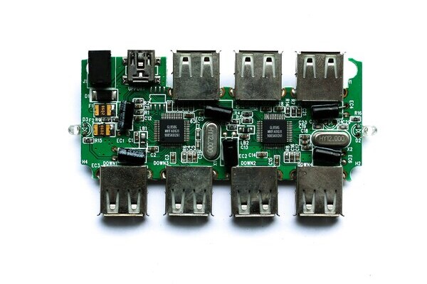
USB PCB Design Components
| Component | Why it matters | Practical design point |
|---|---|---|
| USB connector | Provides the electrical and mechanical interface. | Check footprint, shell tabs, board-edge clearance, and insertion load. |
| ESD protection | Reduces damage from contact discharge. | Place low-capacitance devices close to the connector with a short ground return. |
| CC and PD circuitry | Defines USB-C role and power negotiation. | Even a simple USB-C device needs correct CC implementation. |
| Controller or bridge IC | Handles protocol conversion and product function. | Follow the IC reference layout, especially decoupling and clock placement. |
| VBUS protection | Manages current, surge, and fault conditions. | Size copper and protection parts for real maximum current, not nominal current. |
USB PCB Types
By data rate, USB PCBs range from USB 2.0 boards to USB 3.2 and USB4-class designs. Higher rates demand tighter impedance control, shorter discontinuities, and more careful material and connector choices. By form factor, common products include USB-A interface boards, Micro-USB device boards, USB-C daughterboards, portable SSD enclosure boards, and hub or dock mainboards. Do not infer performance from the connector alone: USB-C is a connector format. It may carry USB 2.0, USB 3.x, charging, or Power Delivery, depending on the complete circuit and cable.
USB PCB Uses and Applications
USB PCBs appear in portable SSDs, flash drives, card readers, programming tools, industrial data acquisition products, keyboards, chargers, and docking products. In an SSD enclosure, the bridge IC converts the NVMe or SATA side to USB. The board must therefore support the high-speed channel, the M.2 connector's mechanical load, the thermal behavior of the controller, and the input current path. In industrial products, ESD performance, common-mode noise, and grounding often deserve priority over a headline maximum transfer rate.
Advantages of a Custom USB PCB
A purpose-built USB PCB combines enclosure dimensions, port orientation, mounting holes, power architecture, and product functions in one controlled assembly. This reduces hand-wiring variation and makes testing and support more repeatable. A documented stack-up and impedance plan also help reduce production variation. More layers are not automatically better: a simple USB 2.0 control board may work well on two layers with a continuous ground reference, while a crowded USB 3.x or SSD design often benefits from four or more layers.
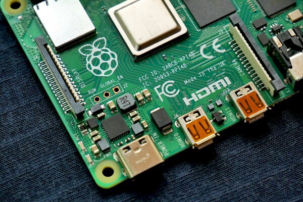
USB PCB Design Requirements
Start with the USB generation and the board-level channel length. USB 2.0 D+ and D? are still a differential pair and should remain together, reasonably length-matched, and referenced to a continuous ground plane. USB 3.x SuperSpeed pairs are more sensitive to vias, stubs, plane changes, and discontinuities. Typical targets are approximately 90 ohms differential for USB 2.0 and 85 ohms differential for SuperSpeed pairs, but the final values must follow the IC, connector, stack-up, and fabricator impedance calculation. Never route a high-speed pair across a split plane or a gap that breaks its return path.
| Area | Recommended approach | Avoid |
|---|---|---|
| Thickness and material | Use standard 1.6 mm FR-4 for many products; select 0.8 or 1.0 mm only when mechanics and stack-up support it. | Choosing thickness from enclosure size without checking connector retention and impedance. |
| Stack-up | Place critical signals adjacent to a solid reference plane; four layers often make return paths easier to control. | Routing above plane splits or changing layers without a nearby ground return via. |
| Routing | Keep differential pairs on one layer and reference plane where possible; minimize vias and branches. | Unequal routing, abrupt geometry changes, or test-point stubs on a high-speed pair. |
| Impedance | Specify target impedance, copper weight, dielectric information, and tolerance in fabrication notes. | Calling out "differential pair" with no impedance target or approved stack-up. |
| Power and ground | Calculate VBUS copper width for worst-case current; keep ESD ground paths short. | Letting high-current return paths interfere with sensitive high-speed signals. |
USB PCB Connector Types
USB-A is established on host-side products but is directional. USB-B remains useful in some equipment applications. Micro-USB is compact but less durable and less convenient than newer options. USB-C supports reversible insertion and can support CC and PD functionality. Selection should also consider rated current, insertion cycles, SMT or through-hole retention, mid-mount dimensions, shell tabs, and sealing requirements. On a frequently handled portable SSD, shell-tab strength, annular ring, board edge clearance, and enclosure support are real reliability features.
USB-C PCB Upgrade and Manufacturing Differences
Moving from a traditional connector to USB-C does not automatically require special PCB fabrication. A USB 2.0 USB-C device with basic power can normally use standard FR-4, standard surface finish, ordinary drill sizes, and conventional layer counts. The practical difference is often denser connector pads and tighter assembly control. Manufacturing requirements change only when the product capability changes: USB 3.x or higher speeds, high-current PD, fine-pitch bridge ICs, and constrained routing may require tighter impedance tolerance, finer features, additional layers, laser vias, or lower-loss material. Define these needs from the actual stack-up and DFM review, not from the USB-C label alone.
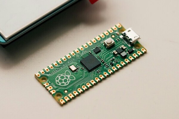
USB PCB Price
USB PCB cost depends on board area, layer count, quantity, material, copper weight, surface finish, controlled impedance, minimum feature size, drill technology, test requirements, and delivery schedule. In prototype quantities, engineering and special-process charges can dominate; in volume, panel utilization and a stable process window have more influence. For a meaningful quotation, provide quantity breaks, finished thickness, finished copper weight, impedance table, surface finish, panel requirements, and lead-time target. An incomplete request can look inexpensive initially but create avoidable cost through later fabrication queries or redesign.
USB PCB Failures and Troubleshooting
Typical symptoms include no enumeration, repeated disconnects, low-speed fallback, reset during insertion, hot power parts, and unstable transfer. Begin with connector soldering and USB-C CC state, then measure VBUS voltage drop and ground continuity. Next, check the differential pairs for opens, shorts, extreme skew, and excessive vias. For high-speed faults, use known-good host and cable combinations and, when available, eye-diagram or error testing; a continuity test alone cannot prove channel quality. If a delivered board shows a fabrication or assembly-related issue, PCBgogo can promptly review order details, defect photos, test conditions, and revision-controlled design files, then coordinate troubleshooting and, where appropriate, rework or repair handling.
Why Choose PCBgogo for Your USB PCB Project
A USB PCB project needs manufacturing collaboration, not generic promises. The practical value lies in checking stack-up and impedance manufacturability before release, identifying conflicts in pads, drill sizes, panelization, and process notes before production, and maintaining a traceable route for post-delivery issues. PCBgogo can support Gerber review, prototype and production manufacturing, impedance and surface-finish options, and communication for rework or repair cases. For a reliable USB PCB, submit the connector area, high-speed routing, power section, and mechanical constraints together; reviewing one isolated differential pair is rarely enough.
PCBgogo - Reliable, High-Quality PCB Manufacturing
Save time and money with an all-in-one solution for PCB fabrication, assembly, and parts. Reduce vendor coordination, avoid split shipments, and get consistent, reliable quality.
Get Free Quote >
Conclusion
A dependable USB PCB begins with a precise product definition and succeeds when signal routing, power delivery, protection, mechanics, and manufacturing documentation agree. For an SSD product, confirm the USB generation, power requirement, and internal storage interface first. Then select the connector, stack-up, and fabrication options, and validate the prototype with insertion, sustained transfer, and thermal tests. That process produces design rules that can be repeated in production.
FAQ
Does every USB PCB need four layers?
No. A short, simple USB 2.0 design may be suitable for two layers with a continuous ground reference. Four layers are often the more robust option for tighter layouts, USB 3.x, or complex power requirements.
Can USB-C directly replace Micro-USB?
No. The footprint is different, and USB-C requires correct CC configuration and role-specific power behavior. Review the schematic, protection, and mechanical design rather than making a connector-only substitution.
Why does a portable SSD USB PCB slow down
Possible causes include negotiated speed fallback, cable loss, bridge-controller thermal throttling, VBUS voltage drop, or excessive high-speed channel loss. Confirm the negotiated link, temperature, and cable/host behavior before changing the PCB.





