
 日本語
日本語
 한국어
한국어

10 Layer PCB Guide: Stackup, Design, Cost & Uses
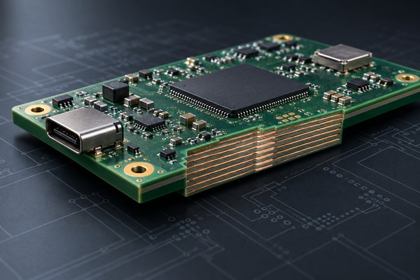
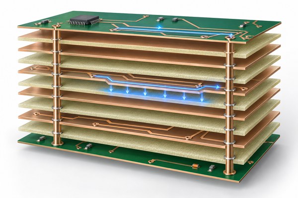
A 10-layer PCB stacks ten conductive copper layers, separated by prepreg and core dielectric, into a single rigid board. Most 10-layer stackups split the layers into four to six for signal routing, with the rest dedicated to ground and power planes, though the exact split depends on the design's routing needs and impedance targets. A common arrangement places each signal layer next to a solid ground plane, so high-speed traces have a continuous return path close by rather than jumping across the board.
Total board thickness usually lands around 1.6 mm (0.062"), matching standard connector and enclosure specs, though thinner or thicker builds are possible depending on copper weight and dielectric choice. The specific stackup — which layers carry ground, where the power planes sit, how thick each dielectric layer is — should be worked out with your fabricator's engineering team rather than copied from a generic template, since material stock and lamination process vary between manufacturers.
Why Design Teams Land on 10 Layers (Not 8, Not 12)
The jump from 8 to 10 layers isn't just about adding more room — it's usually a response to three specific pressures. The first is routing headroom: a BGA with 300 or more balls often can't fan out cleanly on 8 layers without crowding traces or breaking spacing rules, and 10 layers gives just enough extra routing channels to solve it without over-building the board.
The second is signal integrity. High-speed interfaces — DDR3/DDR4, PCIe, Gigabit Ethernet, USB 3.0 — need controlled impedance and a continuous reference plane close to every trace. On an 8-layer board, fitting enough dedicated ground and power planes next to every high-speed signal layer can force compromises. Two extra layers usually resolves that without redesigning the whole floor plan.
The third is cost discipline. Once you're past 8 layers, the real decision isn't 9 versus 11 — it's whether you actually need 12 or more. Each additional layer pair adds lamination cycles, material, and lead time. For most designs with one or two moderate-pin-count BGAs and a handful of high-speed interfaces, 10 layers is the practical ceiling before cost climbs faster than the design actually needs. Very high pin count FPGAs or SoCs, backplanes, and extremely dense mixed-signal boards are the cases where 12+ layers genuinely earns its keep — for most designs pushing past 8 layers, 10 is the more sensible stop.
A useful gut-check: if your routing struggles trace back to one or two BGAs and one or two high-speed interfaces, 10 layers is usually enough headroom. If you're fighting routing congestion across half a dozen high-pin-count components at once, that's a sign the design belongs in the 12+ layer category regardless of cost preference — no amount of clever routing on 10 layers will fix a floor plan that genuinely needs more planes.
Where 10 Layer PCBs Show Up in Real Products
In practice, 10-layer boards cluster around a specific type of design: enough complexity to need serious routing room and impedance control, but not so much that it demands server-backplane-level layer counts.
Automotive electronics are a common example — ADAS modules, EV battery management systems, and engine or motor control units typically combine multiple high-speed sensor and communication interfaces with the thermal and reliability demands of an automotive environment, which makes the extra planes worth the added layers.
Networking and telecom hardware is another — managed switches, small-cell base stations, and routers often need to route multiple high-speed interfaces (Ethernet, PCIe, memory buses) side by side, which is difficult to do cleanly on 8 layers.
Industrial automation equipment, including PLCs, motor drives, and multi-protocol sensor hubs, frequently lands at 10 layers because these boards combine several communication buses with power distribution for onboard drive electronics. Medical devices — portable diagnostic equipment and patient monitors, for example — often need compact, dense routing without the cost of full HDI backplane complexity, making 10 layers a practical middle ground. Test equipment and mid-range computing boards with a couple of moderate-pin-count BGAs and multiple high-speed interfaces round out the list: designs where 8 layers can't fit the routing, but the full complexity of a 16-to-20-plus-layer board isn't warranted.
What Changes in Design and Manufacturing at 10 Layers
Moving to 10 layers changes more than the number on the spec sheet — it changes what your fabricator needs to get right.
Impedance control gets tighter. With more internal planes contributing to a trace's electrical environment, controlled-impedance traces need closer tolerance matching between the fabrication process and the dielectric's actual properties, not just the datasheet numbers.
Via strategy becomes a real decision rather than a formality. Standard through-hole vias work fine for many 10-layer designs, but blind or buried vias — or via-in-pad for dense BGA fields — free up routing space and reduce layer-to-layer conflicts when board space is tight.
Material selection matters more. Dielectric constant (Dk) consistency and glass transition temperature (Tg) become more relevant as layer count and copper weight increase, particularly for automotive and industrial boards that see thermal cycling in the field.
Lamination gets more complex. More layers — and especially blind or buried via structures — mean more lamination cycles, which can extend lead time compared to a straightforward 4- or 6-layer build.
Inspection matters more, not less. Shorts and opens on internal layers aren't visible from the outside, so AOI at multiple stages and X-ray inspection for buried via structures move from "nice to have" to standard practice for catching defects before they reach assembly.
What to Ask Before Choosing a 10 Layer PCB Manufacturer
A 10-layer board has enough complexity that the fabricator you choose matters more than it did for a simple 2- or 4-layer job — a stackup error or a missed via-in-pad requirement is far more expensive to fix after lamination than before it. A few questions worth asking before committing:
Layer count headroom: can they comfortably go beyond 10 layers if a later revision needs it, rather than being at the edge of their own capability?
Material options: do they offer laminates suited to your Tg and dielectric requirements, not just a single default FR-4?
DFM review: does someone check your stackup and via structure before production, or does the board go straight to the line as submitted?
Inspection process: is AOI and X-ray inspection standard for multilayer boards, or an added-cost option?
Fabrication and assembly under one roof: will you be coordinating a separate fab house and assembly house, or can one vendor carry the board from bare PCB to populated assembly?
How PCBgogo Fits Into a 10 Layer PCB Build
PCBgogo fabricates multilayer boards well beyond the 10-layer range — up to 40 layers — so a 10-layer design has plenty of headroom if a later revision adds layers or density. Boards are built on Shengyi and Kingboard substrates, laminate choices suited to the Tg and CAF-resistance requirements that automotive and industrial 10-layer designs typically call for.
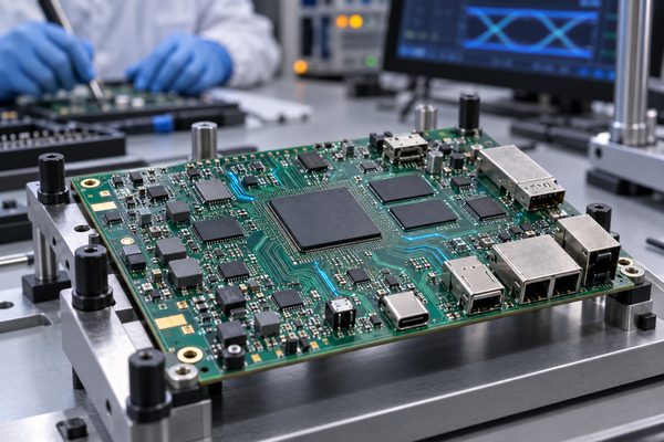
Every order goes through a DFM/engineer review before it enters production, and internal layers are checked with AOI and X-ray inspection to catch defects that aren't visible from the outside once the board is laminated. For projects on a tighter deadline, PCBgogo offers 24-hour quick-turn options alongside standard lead times.
Because fabrication and assembly run in the same facility, a 10-layer board can move from bare PCB to populated assembly without switching vendors or re-verifying files partway through the process. Native Eagle, Altium, and PADS files are accepted alongside Gerbers, so design teams don't have to convert files just to get a quote.
Layer count, via structure, and material choice all affect price and lead time in ways specific to your stackup, so the most accurate way to see where a 10-layer design lands is to run the actual specs through PCBgogo's online quoting tool rather than relying on a general estimate. Submit your stackup for free DFM review from PCBgogo engineers
PCBgogo - Reliable, High-Quality PCB Manufacturing
Save time and money with an all-in-one solution for PCB fabrication, assembly, and parts. Reduce vendor coordination, avoid split shipments, and get consistent, reliable quality.
Get Free Quote >
Frequently Asked Questions
What is a 10-layer PCB used for?
10-layer PCBs are typically used in automotive ECUs, networking equipment, industrial controllers, and medical devices that need more routing room and better impedance control than an 8-layer board can offer, without the cost of a 12-layer design.
Is a 10 layer PCB more expensive than an 8 layer PCB?
Yes — added layers mean more lamination cycles and material, which raises cost and lead time compared to an 8-layer board, though the exact difference depends on your specific stackup and via structure.
Does a 10 layer PCB require blind or buried vias?
Not necessarily. Many 10-layer designs use standard through-hole vias, and blind or buried vias are typically added only when BGA fan-out or tight space constraints make routing difficult otherwise.
What's a typical lead time for a 10 layer PCB?
Lead time depends on stackup complexity and via structure, but most 10-layer boards fall between standard multilayer turnaround and quick-turn options — worth checking directly if you're working against a deadline.
Do I need HDI technology for a 10 layer PCB?
No. HDI refers to via technology, such as microvias and sequential lamination, not layer count — a 10-layer board can be built as a standard multilayer PCB or as an HDI board depending on routing density.
What files does a manufacturer need to fabricate a 10 layer PCB?
Most fabricators need Gerber files along with drill files and stackup information, and many manufacturers, including PCBgogo, also accept native Eagle, Altium, or PADS files directly.





