



 日本語
日本語
 한국어
한국어

Standard PCB Thickness Guide: How Thin Can Your Board Really Go?
QUICK ANSWER Most rigid PCBs use a standard thickness of 1.6mm, though the full range runs from about 0.2mm to 3.2mm depending on layer count and application. The thinnest boards manufacturers can reliably produce sit around 0.2mm for one or two layers, while multilayer designs need more material and rarely drop below 0.6mm to 1.0mm.
Pick up almost any consumer gadget and crack it open, and there's a good chance the board inside measures 1.6mm thick. That's not a coincidence. It's a number the industry settled on decades ago, and most designers never think to question it until a project demands something thinner, thicker, or just different.
This guide breaks down what standard PCB thickness actually means, how thin a board can realistically go, and what should drive your decision either way.
What Counts as Standard PCB Thickness
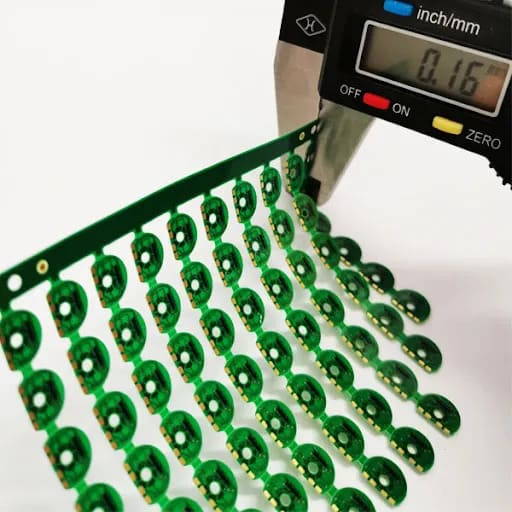
Standard PCB thickness refers to 1.6mm, or 0.063 inches, the default value most fabricators use unless a design specifically calls for something else. The number traces back to early circuit boards built on plywood substrates, where a single ply measured close to 1.57mm. That figure stuck as connectors, card edge slots, and enclosure tolerances standardized around it, and it remains the value most fabrication lines are tuned for today.
But "standard" isn't fixed. The available range shifts with layer count, since a two-layer board and a ten-layer board draw on very different amounts of copper and dielectric material to hit the same nominal thickness.
| Layer Count | Common Thickness Range | Typical Use |
|---|---|---|
| 1 to 2 Layers | 0.2mm to 2.4mm | Simple consumer devices, sensors, badges |
| 4 Layers | 0.4mm to 2.4mm | Routers, small controllers, IoT modules |
| 6 to 8 Layers | 0.8mm to 2.4mm | Communication equipment, servers |
| 10+ Layers | 1.2mm and up | High density networking, industrial systems |
Boards with fewer layers can go thinner because there's simply less internal material to stack. Once you're past eight or ten layers, the copper and dielectric needed for routing and impedance control set a practical floor on how thin the finished board can be.
How Thin Can a PCB Actually Get
The minimum PCB thickness a fabricator can reliably produce depends far more on layer count than on ambition. For rigid one or two-layer boards, 0.2mm is close to the practical floor, since the substrate still needs enough rigidity to survive drilling, plating, and handling without cracking. Push a multilayer board toward that same number and the odds of warpage or delamination climb fast.
A handful of factors set where that floor actually sits for a given design.
Substrate rigidity: Below roughly 0.2mm, FR4 starts to flex enough during handling and reflow that boards can crack or bow before they ever reach a customer.
Layer count and material buildup: Every additional copper layer adds prepreg and core material, which raises the minimum achievable thickness even if the design would otherwise support something thinner.
Drilling aspect ratio: Thinner boards make small via drilling easier, but very thin multilayer stacks can push the ratio of hole depth to diameter outside what mechanical or laser drilling can plate reliably.
Panelization and handling: Boards under about 0.4mm often need special panel support during SMT assembly, since standard conveyor and pick-and-place equipment isn't built for that much flex.
If your design is pushing toward the thin end, it's worth confirming the number with your fabricator before finalizing the stackup rather than assuming a spec sheet minimum will hold for your specific layer count.
Where Different Thicknesses Actually Show Up
The right board thickness usually falls out of the product it's going into, since space, weight, and mounting hardware set hard constraints before signal performance even enters the conversation.
Wearable trackers and hearing aids: These lean on boards under 0.6mm, often flexible or rigid-flex, where every fraction of a millimeter affects comfort and fit.
Smartphone and tablet motherboards: Most fall in the 0.8mm to 1.2mm range, balancing enough rigidity to survive assembly against the internal space budget of a slim enclosure.
Router and network switch baseboards: These commonly sit at 1.6mm, since they carry enough layers for signal routing while still fitting standard connector and mounting hardware.
Automotive control modules: Boards here often run 1.6mm to 2.0mm, chosen for resistance to vibration and the thermal cycling that comes with under-hood or cabin placement.
Power supply and industrial control boards: These frequently go to 2.0mm or beyond, where the extra thickness supports heavier connectors, higher current traces, and larger heat sinks.
Once the application narrows the general range, the next question is what specifically inside that range is worth optimizing for.
What Actually Drives the Right Thickness Decision
Choosing a thickness isn't really about picking a number from a chart. It comes down to which constraint in your design is least flexible.
Connector and edge mating requirements: Card edge connectors, PCIe slots, and SODIMM-style interfaces are built around 1.6mm or 1.0mm boards, so a design using one of these effectively has its thickness decided for it.
Copper weight and current load: Higher current traces need thicker copper, and thicker copper on the outer layers pushes the practical minimum board thickness up along with it.
Impedance and signal integrity: In high-speed designs, board thickness sets the dielectric spacing between signal and reference planes, which directly shapes controlled impedance and how much attenuation a trace introduces.
Mechanical stress and vibration: Boards that get handled roughly, mounted vertically, or exposed to vibration benefit from added thickness for stiffness, independent of what the electrical design would otherwise call for.
Panel size and warpage risk: Larger boards are more prone to warping during reflow, and a thicker substrate helps resist that bow across a bigger panel.
Weighing these against each other, rather than defaulting straight to 1.6mm, is what actually separates a considered spec from a placeholder one.
What PCB Thickness Tolerance Actually Means
Thickness tolerance isn't a single number. It's usually expressed as a percentage for thicker boards and a fixed value for thinner ones, since a flat percentage on a 0.2mm board would leave almost no usable margin.
IPC's board fabrication standards, which most manufacturers reference for classifying acceptable variation, split tolerance this way precisely because the manufacturing risk at the thin end isn't proportional to the nominal thickness. A board specified at 2.0mm can absorb a wider absolute swing than one specified at 0.4mm, even though both might carry a similar percentage tolerance on paper.
It also helps to know what that tolerance does and doesn't cover. The number describes the finished bare board, including copper, solder mask, and any surface finish, not just the raw substrate before processing. That's part of why a board can come in slightly over its nominal spec even when nothing went wrong in production.
How PCBgogo Handles Thickness Across Layer Counts
Once you know roughly where your design needs to land, the next question is whether a fabricator can actually hit that number consistently across the layer count you're using.
Thickness scales with your layer count, not a fixed catalog: PCBgogo's FR-4 capabilities run 0.2mm to 2.4mm on 1 and 2 layer boards, 0.4mm to 2.4mm on 4 layer boards, and up to 1.2mm and beyond on 10 layer boards, with custom stackups available outside that range on request.
Tolerance held to the same split logic: boards at 1.0mm and above hold ±10%, while anything under 1.0mm is controlled to a fixed ±0.1mm, so thin boards aren't stuck with a percentage tolerance that would be meaningless at that scale.
TG grade matched to the application: standard TG130 for general electronics, up to TG170 for automotive or high temperature builds, using Shengyi laminates across the range.
Per order DFM review: every stackup and thickness combination gets checked by an engineer before fabrication starts, which catches issues like an aspect ratio that won't plate reliably before the board goes into production rather than after.
If you're not sure which thickness fits your specific stackup, PCBgogo's instant quote tool will flag any spec that falls outside standard capability before you commit to an order.
Frequently Asked Questions
What is the standard thickness of a PCB?
The standard PCB thickness is 1.6mm, the default most fabricators use unless a project specifies otherwise. It became the industry norm because it balances mechanical strength, connector compatibility, and manufacturability for the widest range of applications.
What is the minimum PCB thickness a manufacturer can produce?
For rigid one or two-layer boards, around 0.2mm is the practical minimum most fabricators can reliably hold. Multilayer boards need more material to route and insulate properly, so their realistic floor is closer to 0.6mm to 1.0mm.
Does more layers always mean a thicker board?
Not necessarily at the low end, but the minimum achievable thickness does rise with layer count. A 10-layer board simply can't be made as thin as a 2-layer board because of how much copper and dielectric material each additional layer requires.
How does PCB thickness affect cost and lead time?
Standard thicknesses like 1.6mm are typically the fastest and most cost-effective to produce, since they match a fabricator's default process setup. Nonstandard thickness values, especially very thin or very thick ones, often add lead time for stackup review and process adjustment.
What thickness should I use for automotive or high current boards?
Most automotive and high current designs land between 1.6mm and 2.0mm, which supports heavier copper weights and better resists vibration and thermal cycling. The exact number still depends on connector requirements and the specific current the board needs to carry.
Can I request a custom PCB thickness?
Yes, most fabricators support custom thickness outside their standard range, though it typically requires a stackup review before the order is confirmed. Expect a longer lead time compared to ordering a standard value like 1.6mm or 0.8mm.
The Bottom Line
Standard PCB thickness gives you a safe, fast, cost-effective default at 1.6mm, but it isn't the right answer for every project. The real decision comes down to layer count, connector requirements, and how much mechanical or thermal stress the board needs to survive, with tolerance and manufacturability setting the outer limits either way.





