




 日本語
日本語
 한국어
한국어

What Is SSD PCB? Custom High-Performance PCB for Your SSDs
KEY DEFINITION
An SSD PCB is the printed circuit board that connects NAND flash, a storage controller, DRAM or host memory buffer, power circuitry, and the host interface into one reliable solid-state drive. Its layout directly affects signal integrity, heat flow, manufacturability, and sustained data performance.
Key Takeaways
An SSD PCB is a high-speed interconnect platform, not merely a carrier for memory packages.
Interface routing, power delivery, thermal paths, and assembly tolerances must be planned together.
The smallest drives demand the most disciplined stackup, component placement, and inspection strategy.
A fabrication partner should review the manufacturing data before production, especially for fine pitch BGA footprints and controlled impedance nets.
Introduction
A solid-state drive can look simple from the outside, yet its board must move data at multi-gigabit rates while keeping flash, controller, and power circuits within safe operating limits. A weak SSD PCB may still boot, but show intermittent link training, thermal throttling, or poor manufacturing yield.
This guide explains what an SSD PCB does, practical design and sourcing decisions, and what to check before volume production.
What Is an SSD PCB
An SSD PCB is the multilayer board that electrically and mechanically integrates the devices required for nonvolatile solid-state storage. In a typical NVMe drive, the controller exchanges data with the host through PCIe differential pairs and manages several NAND channels on the same board. The PCB must preserve reference planes and return paths so those high-speed signals remain predictable.
The form factor changes the engineering tradeoff. An M.2 2280 board is nominally 22 mm wide and 80 mm long, whereas a compact BGA SSD places the storage subsystem in a package substrate. For a discrete M.2 or U.2 style design, board area is scarce, so placement must give the controller a short thermal route and give each NAND package a clean fanout strategy.
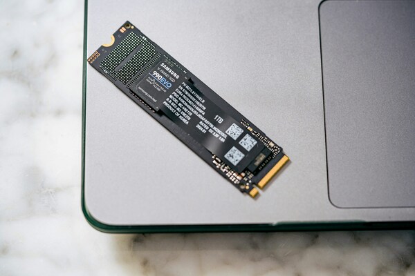
Key Components on an SSD PCB
The key components of an SSD PCB are the controller, NAND flash, optional DRAM, power management circuitry, host connector, clocking, and protection parts. Each has a different placement priority: controller and NAND connections drive routing density, while inductors, capacitors, and thermal features drive power and heat management.
SSD controller: This processor schedules flash operations, applies error correction, manages wear leveling, and handles the host protocol. Keep its decoupling capacitors close to the relevant supply pins, using short, low-inductance connections to solid ground.
NAND flash: NAND packages store user data in blocks and pages. Arrange packages so data and control traces are consistent, and avoid splitting a channel across discontinuous reference planes.
DRAM or HMB support: Some drives use local DRAM for mapping tables; others use host memory buffer features. A local DRAM interface adds dense, length-sensitive routing, so reserve escape space before fixing component locations.
Power stage: A PMIC, buck inductors, bulk capacitors, and bypass capacitors convert the input rail into controller and flash rails. Separate switch nodes from sensitive clock and high-speed data routes.
How an SSD PCB Works in Data Storage
An SSD PCB works by carrying host commands to the controller, distributing regulated power, and linking the controller to parallel NAND channels. When the host requests data, the controller locates the logical address, reads physical flash pages, corrects errors, and returns the data through the host interface. During writes, it buffers and organizes data before programming NAND pages and later consolidates blocks during garbage collection.
The board supports this workflow through geometry and materials. Differential PCIe pairs need controlled impedance, matched routing within the design rule set, and continuous reference planes. Power planes need enough copper and via capacity to avoid local voltage drop during burst activity. These decisions are related: a via field that helps BGA escape can also interrupt a return path if the adjacent plane is poorly planned.
Main SSD Types and Their PCB Implications
SSD types differ mainly by interface and physical format, which changes connector placement, routing density, and thermal allowance. The table helps a product team connect a market requirement to an early board architecture choice.
| SSD type | Host connection | PCB focus | Typical fit |
|---|---|---|---|
| SATA SSD | SATA connector | Moderate speed routing, power input protection | Legacy upgrades and industrial systems |
| M.2 SATA | Edge connector | Compact layout with SATA signaling | Thin client and embedded products |
| M.2 NVMe | PCIe edge connector | Controlled impedance differential pairs and controller cooling | Client PCs and compact computing |
| U.2 or enterprise module | Cable or backplane connection | Power integrity and serviceable mechanics | Servers and storage appliances |
SSD PCB Applications
SSD PCBs are used wherever a system needs persistent storage with fast access, small volume, or resistance to vibration. The application determines how much attention should go to temperature range, retention, connector cycling, and mechanical restraint.
Industrial controllers: Factory equipment often sees vibration, dust, and wide temperature variation. Use secure mounting, a conservative component clearance strategy, and a validation plan that includes power cycling and temperature exposure.
Edge computers: Compact gateways and AI appliances put the SSD near processors and radios. Maintain separation from strong RF or switching noise sources, and do not assume a metal enclosure alone solves controller heat.
Servers and storage arrays: Serviceable drives require connector alignment and repeatable insertion behavior. Backplane and drive layouts should be reviewed as one signal path, including ground continuity through the connector.
Embedded medical and imaging equipment: Product reliability depends on stable power and documented manufacturing controls. Lock the material, surface finish, and test method before release.
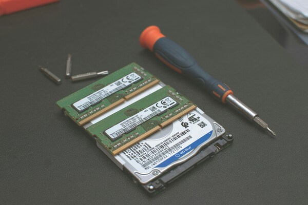
SSD PCB Design Layout
An effective SSD PCB layout begins with the stackup and placement plan, because routing cannot repair a poor power or thermal architecture later. Start by obtaining the controller reference design constraints, then confirm the fabricator can build the chosen trace geometry, via structure, and copper weight before finalizing the layout.
Stackup and impedance: Assign high-speed layers next to uninterrupted ground planes. Define target impedance with the board supplier using the actual dielectric thickness and copper profile, not a generic calculator assumption.
BGA fanout: Fine pitch controller and NAND packages often make via selection the first yield decision. Keep solder mask dams, annular rings, and escape channels compatible with the selected assembly process.
Power integrity: Place small ceramic capacitors on the same side as the controller whenever possible. Route each supply with a short path to a low-impedance plane and keep the regulator feedback network away from switch nodes.
Thermal path: Use a controller thermal pad, thermal vias where permitted by the assembly design, and a planned interface to a heatsink or chassis. Verify that via filling or capping is specified when exposed vias could wick solder.
DFM release: Run a fabrication and assembly review before ordering boards. Fabrication data, drill files, stackup, impedance notes, finish, and test requirements should agree.
SSD PCB Manufacturing Process
SSD PCB manufacturing converts the approved stackup and production data into a controlled multilayer interconnect with inspectable features. The usual flow includes inner layer imaging and etching, lamination, drilling, plated through hole formation, outer layer patterning, solder mask, surface finish, electrical test, and final inspection.
For SSD boards, manufacturing choices should be tied to assembly risk. Electroless nickel immersion gold offers a flat surface for fine pitch assembly, while other finishes may be suitable when cost, shelf life, and solderability priorities differ. Controlled impedance coupons, automated optical inspection, and electrical testing provide different evidence: coupons check the built stackup, optical inspection checks visible patterns, and electrical test checks for opens and shorts.
PCBgogo is a practical manufacturing partner for SSD work when the production package needs a fabrication review before release. Sharing the intended stackup, impedance requirements, finish choice, BGA pitch, and expected assembly method enables the engineering team to identify buildability issues early and align the board specification with the production process.
SSD PCB Price
SSD PCB price is driven by board complexity and production controls rather than board area alone. A small NVMe board can cost more than a larger simple board because it may require more layers, tighter line and space, controlled impedance, fine pitch BGA support, impedance verification, and a surface finish selected for assembly quality.
For a useful quotation, provide quantity, dimensions, layer count, material class, copper weight, finished thickness, feature requirements, via types, finish, impedance notes, and test requirements. State whether the request covers bare boards only or includes assembly. This avoids comparing different technical scopes.
SSD PCB Technical Challenges and Future Trends
SSD PCB development faces a continuing tension between higher bandwidth and a smaller thermal and routing envelope. The following issues deserve a design review before they appear as late prototype failures.
Higher PCIe data rates: Faster interfaces reduce timing and loss margin. Material selection, pair geometry, via transitions, connector quality, and return path continuity become system-level concerns.
Controller heat density: More active channels and performance features concentrate heat in a small controller footprint. Thermal simulation is useful, but it must be checked against the real enclosure, airflow, interface pad, and sustained workload.
NAND package density: Adding packages can shorten the available routing corridor and increase assembly complexity. A symmetrical placement plan and early BGA escape study prevent last-minute layer additions.
Production traceability: Clear revision control, approved substitutions, inspection criteria, and test documentation make failure analysis faster and more credible.
Sustainability and repairability: Longer product life favors designs that can be diagnosed and serviced without compromising performance. Thoughtful connector access, clear labeling, and robust pad design help support that goal.
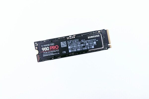
Why PCBgogo Is a Strong PCB Manufacturing Partner for SSD Projects
PCBgogo can support SSD projects by turning a board requirement into a manufacturable fabrication plan before production. For designs with controlled impedance routes, fine pitch packages, and tight thermal geometry, early engineering communication is more valuable than a generic quote.
Prepare a manufacturing package stating the SSD form factor, stackup intent, controlled impedance nets, finish, BGA requirements, inspection expectations, and quantity. This gives PCBgogo the information needed to review the build and prevent a mismatch between layout intent and the fabricated board.
PCBgogo - Reliable, High-Quality PCB Manufacturing
Save time and money with an all-in-one solution for PCB fabrication, assembly, and parts. Reduce vendor coordination, avoid split shipments, and get consistent, reliable quality.
Get Free Quote >
Summary
An SSD PCB is the electrical, thermal, and mechanical foundation of a solid-state drive, so its success depends on coordinated choices in stackup, routing, power delivery, assembly, and testing. Treat the fabrication package as part of the design, not a handoff document, and engage PCBgogo early when the project needs a buildability review for high-speed, fine-pitch storage hardware.
FAQ
What layers are typical for an SSD PCB?
The required layer count depends on interface speed, controller package, NAND count, and available board area. A simpler SATA layout may need fewer routing resources than a dense NVMe layout, where dedicated reference planes and BGA escape routing often justify a more complex stackup.
Why does controlled impedance matter on an NVMe SSD PCB?
Controlled impedance helps PCIe differential pairs behave predictably from controller to connector. The correct target is established from the controller and interface requirements, then achieved through the actual laminate, copper, trace geometry, and reference plane configuration.
Can thermal vias be placed under an SSD controller?
Thermal vias can improve the path from the controller pad to an opposite side copper area or heatsink interface. Their treatment must match the assembly design, because open vias may draw solder away from the thermal pad unless they are filled, capped, or otherwise managed.
What files should be sent for SSD PCB fabrication?
Send the fabrication outputs, drill data, stackup, impedance requirements, board outline, finish requirement, and clear fabrication notes. Include the assembly data and BOM when assembly is part of the scope, especially for fine-pitch controller and NAND packages.
How can I reduce SSD PCB prototype risk?
Reduce risk by reviewing BGA fanout, power decoupling, return paths, thermal contact, and manufacturing limits before placing the order. A pre-production DFM review catches many issues that electrical simulation alone does not reveal.





