



 日本語
日本語
 한국어
한국어

What Is Solder Mask in PCB Manufacturing? PCBgogo Complete Guide
Every board that leaves a fabrication line carries a thin polymer skin most engineers never think twice about, until it fails. PCB solder mask is that skin, and getting it wrong is one of the fastest ways to turn a clean design into a field return. I have spent years reviewing fabrication drawings, chasing down solder bridging complaints, and rejecting Gerber files for mask clearances that looked fine in the CAD tool but were unmanufacturable on a real panel. This guide covers what the design rule tables leave out.
What Is PCB Solder Mask?
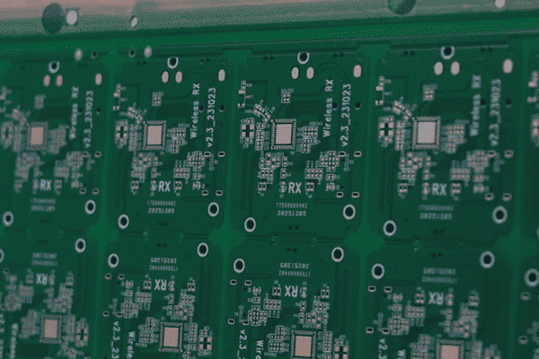
PCB solder mask is a thin, permanent polymer coating applied over the copper layers of a printed circuit board, leaving only the pads, vias, and other bondable features exposed. Its job is to insulate the copper traces from the environment and from each other, and to define exactly where solder is allowed to flow during assembly.
Solder mask is not paint. It is a dielectric layer with real electrical, thermal, and mechanical properties: dielectric strength, glass transition behavior, chemical resistance, and adhesion to copper. On a finished board, mask typically covers 80 to 95 percent of the surface area, so its quality has an outsized effect on long-term reliability.
A useful mental model: solder mask is a negative image. Wherever the mask artwork has a pattern, ink is removed and copper is exposed. Wherever there is no pattern, ink stays and the copper underneath stays covered. Designers sometimes get this backwards on their first few layouts, then wonder why unexpected copper is exposed on the finished board.
Why Solder Mask Matters: The Five Functions
1. Prevents solder bridging. During reflow or wave soldering, molten solder will wet any exposed copper it touches. Mask confines solder to intended pads, which is the single biggest defect-prevention function it serves.
2. Protects against corrosion and oxidation. Exposed copper reacts with moisture, sulfur compounds, and airborne contaminants. The mask keeps traces sealed against humidity and chemical attack over the product's service life.
3. Provides electrical insulation between adjacent conductors. At fine pitch, unmasked copper features close together can allow leakage current or, in humid conditions, dendritic growth that eventually shorts the circuit.
4. Adds mechanical and dielectric protection. Mask reduces the chance of scratches breaching the copper and raises the breakdown voltage of the surface dielectric stack.
5. Enables visual inspection and branding. Silkscreen legend sits on top of mask, and mask color affects how easily automated optical inspection (AOI) systems and human inspectors can see trace geometry, solder joints, and defects.
How Solder Mask Is Manufactured: The Real Process Flow
Understanding the process explains almost every design rule that follows.
Step 1: Surface preparation. After copper etching, the panel is scrubbed and micro-etched to remove oxides and roughen the copper surface, which is what gives the mask ink something to mechanically key into. Skipping or under-running this step is a leading cause of mask delamination months later, not at incoming inspection.
Step 2: Ink application. Liquid photoimageable (LPI) mask is applied by curtain coating, screen printing, or spray coating, then vacuum laminated or roller coated for dry film variants. Coating thickness is controlled here and directly affects both appearance and the achievable minimum dam width.
Step 3: Pre-bake (tack cure). The panel goes through a low-temperature bake to drive off solvents and firm up the ink without fully curing it, so it can still be selectively exposed.
Step 4: UV exposure. A phototool (or direct laser imaging, LDI) exposes the panel to UV light through a mask pattern. Exposed ink cross-links and hardens; unexposed ink stays soluble. LDI has largely replaced film phototools on modern lines because it removes registration error introduced by film stretch and eliminates dust and scratches on physical film.
Step 5: Development. The panel is run through a mildly alkaline developer that washes away unexposed, uncured ink, revealing bare copper where pads and features belong.
Step 6: Final cure. A high-temperature bake (typically 150°C or higher) fully cross-links the remaining ink, giving it its final chemical resistance, hardness, and adhesion strength.
Step 7: Surface finish. Only after the mask is fully cured does the board proceed to surface finish, ENIG, HASL, immersion silver, OSP, or similar, which is applied exclusively to the exposed copper the mask has defined.
The reason I walk through all seven steps is that most solder mask defects trace back to one of them, not to the final inspection step where they get caught.
Solder Mask Design Rules Every Engineer Should Know
Solder Mask Expansion (Swell)
Mask openings are drawn larger than the copper pad to tolerate layer-to-layer registration error during fabrication. This is called solder mask expansion or swell. A typical expansion is 0.05 to 0.1 mm (2 to 4 mil) per side, meaning the finished opening is 0.1 to 0.2 mm larger overall than the pad. If you need an opening that matches the pad exactly, you must state it explicitly in your fabrication notes; otherwise the fabricator applies their standard expansion by default, which can visibly change pad geometry on pads that sit on wide copper planes.
Minimum Solder Mask Dam (Web) Width
The dam is the sliver of mask left between two adjacent solder mask openings, for example between the pads of a fine-pitch QFN or between a pad and a via. This is usually the tightest constraint on a dense layout, tighter than trace-to-trace spacing in many designs.
Industry-standard minimums run 0.10 to 0.127 mm (4 to 5 mil) for green mask and slightly wider, roughly 0.127 mm (5 mil), for non-green colors, because pigments other than the traditional green formulation are typically less UV-transparent and require a wider dam to develop cleanly without ink flaking off during the wash step. Go below the minimum and you risk a dam that lifts during development, leaving two pads electrically bridged by exposed copper, exactly the defect the mask was supposed to prevent.
Dam width is a function of ink chemistry, coating thickness, and exposure energy, not just a fixed number, which is why capable fabricators can sometimes push tighter dams than the generic rule of thumb, and why it is worth confirming your fabricator's actual capability rather than designing to the most conservative published figure.
Solder Mask Thickness
Standard LPI mask thickness runs roughly 10 to 20 microns (0.4 to 0.8 mil) over copper traces, thinner over trace edges and corners where the ink naturally recedes. Thickness is not a cosmetic spec:
Too thin, and copper edges at trace corners can show through, risking localized oxidation and reduced dielectric withstand.
Too thick, especially over high copper density areas, and the ink can trap solvent, leading to pinholes or a mask surface that interferes with fine-pitch component seating and solder wetting.
For high-voltage or high-reliability boards, mask thickness contributes measurably to surface creepage and dielectric withstand, so it belongs in your stackup review, not just your DFM checklist.
Tented, Plugged, and Open Vias
Tented vias: mask covers the via without filling the barrel. The lowest-cost option, adequate for vias that do not need to carry solder paste or be probed.
Plugged (mask-filled) vias: resin or mask ink fills the barrel, then is capped. Used where a flat, sealed surface is needed, for example under a BGA where an open via could wick solder paste away from an adjacent pad.
Epoxy-filled and capped vias: filled with non-conductive or conductive epoxy and planarized, used for via-in-pad designs on HDI boards where a component pad sits directly over a via.
Open (untented) vias: intentionally left unmasked, typically for test points or thermal vias where airflow or probe access matters more than sealing.
Choosing the wrong via treatment is a common, quiet cause of assembly yield loss. Via-in-pad on a BGA footprint without proper filling is one of the most frequent root causes I've traced back through a solder-void failure analysis.
Solder Mask Defined vs. Non-Solder Mask Defined Pads
NSMD (non-solder mask defined): the mask opening is larger than the copper pad, so the pad's final shape is set by the copper etch, not the mask. This is the default and preferred approach for most SMT pads, including BGA footprints, because it gives a more consistent solder joint fillet and is more forgiving of mask registration error.
SMD (solder mask defined): the mask opening is smaller than the copper pad, so the mask itself defines the final exposed pad shape. This is occasionally used on very fine-pitch BGAs to add mechanical anchoring for the pad, but it makes the finished pad size directly sensitive to mask registration tolerance, which is a harder variable to control than copper etch tolerance.
Mixing the two conventions inconsistently across a single BGA field is a design review flag I raise constantly. Pick one convention per component family and hold it.
Solder Mask Materials and Application Methods
| Type | Method | Typical Use | Relative Cost |
|---|---|---|---|
| Epoxy Liquid (Screen Printed) | Silkscreen mesh, thermal cure | Low-density, low-cost boards | Lowest |
| Liquid Photoimageable (LPI) | Curtain coat or spray, UV exposure, develop | Vast majority of modern rigid PCBs | Moderate |
| Dry Film Photoimageable | Vacuum lamination, expose, develop | High-density boards, avoids flooding through-holes | Moderate to high |
| Direct Legend / Inkjet Mask | Piezoelectric jetting, no phototool | Prototype and quick-turn runs, lower waste | Moderate |
LPI dominates production PCB manufacturing today because it delivers the resolution needed for fine-pitch dams at a cost that scales well across volumes. Dry film is reserved mostly for very high density interconnect (HDI) work where controlling ink flow into microvias matters more than cost. Direct-imaged inkjet mask is gaining ground on prototype and low-volume lines because it skips phototool generation entirely, which shortens lead time, though most volume production still runs LPI with LDI exposure for the registration accuracy.
Solder Mask Color: More Than Aesthetics
Color is a functional decision, not just a branding choice.
Green: the historical default. Best UV transparency of common pigments, which gives it the tightest achievable dam width and the most forgiving development window, and the largest base of process data behind it.
Matte (soft) green: reduces glare under bright assembly-line lighting and camera-based AOI, popular on boards inspected heavily by machine vision.
Black: visually striking and common on consumer products, but it gives the lowest contrast between traces and background, which makes visual and AOI inspection harder and can hide silkscreen legibility issues.
White: mostly reserved for LED and lighting boards, where maximizing reflected light output matters more than trace visibility.
Red, blue, yellow: close in UV transparency to green and commonly used for product differentiation, revision tracking across prototype iterations, or brand color matching.
Purple, gray, transparent (clear): less common, chosen for specific optical or inspection requirements; transparent mask, in particular, offers strong resolution because it does not need to block light for imaging in the same way pigmented inks do.
A detail competitor articles rarely mention: color also interacts with dam width capability. Fabricators generally publish a wider minimum dam for non-green colors because most pigments other than green absorb more UV energy, which slows and complicates full-depth cure at the ink-to-copper interface on a narrow dam. If your layout is dam-limited, confirm your color choice against your fabricator's actual color-specific capability table before you lock the palette, not after boards come back with lifted dams.
PCBgogo, for reference, controls solder mask ink thickness to IPC Class 2 standards and offers eleven mask colors: green, red, yellow, blue, white, matte green, black, matte purple, purple, gray, and transparent, giving designers latitude to match inspection, thermal, and branding requirements without defaulting to the generic green-only assumption many shops still push.
IPC Standards Governing Solder Mask
IPC-SM-840: the primary qualification and performance specification for solder mask materials. It sorts materials into telecommunications-grade (Class T) and high-reliability/military-grade (Class H) categories, with defined test methods for adhesion, hardness, flammability, thermal shock, and chemical resistance.
IPC-6012: the end-product acceptability standard for rigid PCBs, referencing solder mask coverage, adhesion, and registration under section 3.7, sorted into Class 1 (general consumer), Class 2 (dedicated service, most industrial and commercial electronics), and Class 3 (high reliability, where continuous performance is required).
IPC-A-600: the visual acceptance criteria standard used by inspectors to judge mask voids, misregistration, and other cosmetic-versus-functional defects.
Class 2 is the practical default for the overwhelming majority of commercial and industrial electronics; Class 3 tightens tolerances further and is reserved for aerospace, medical implantables, and similarly critical applications where a mask defect is not an acceptable risk at any volume.

Common Solder Mask Defects and How to Prevent Them
I have pulled every one of these off a real failure analysis report at some point.
1. Mask flaking or peeling. Root cause is almost always inadequate copper surface roughening before ink application, or full-cure bake temperature or time falling short. Prevention: confirm your fabricator runs a controlled micro-etch step and monitors final cure oven profiles, not just visual inspection after cure.
2. Dam lifting between fine-pitch pads. Caused by designing dams below the fabricator's real capability for the chosen color, or by underexposure during LDI imaging. Prevention: design to your specific fabricator's published dam-width-by-color table, and request a first-article inspection report on dense QFN or BGA fields before committing to volume.
3. Mask misregistration. Mask pattern shifts relative to the copper pattern, exposing unintended copper at pad edges or partially covering pads. Root cause is usually phototool stretch on older film-based lines, which is why LDI-equipped fabricators generally hold tighter registration. Prevention: specify your registration tolerance requirement on the fab drawing and confirm the fabricator's exposure method.
4. Solder mask pinholes. Trapped solvent or air bubbles during coating leave microscopic voids that let moisture or flux residue reach copper. Prevention: adequate pre-bake dwell time and controlled coating thickness; this is a process control issue on the fabricator's side, but it correlates with rushed quick-turn runs, so build in inspection time if your board is high reliability.
5. Color-dependent underexposure. Non-green colors cured with exposure energy tuned for green can come out under-cured at dam edges, which looks fine cosmetically but fails adhesion testing. Prevention: this should be caught by the fabricator's incoming process control, but it is worth asking directly whether exposure parameters are color-specific at your chosen shop.
6. Solder mask on pads meant to be exposed, or vice versa. Almost always a Gerber-to-artwork translation error, commonly from mixing up the solder mask layer polarity or forgetting a layer during export. Prevention: always review the fabricator's DFM report and, ideally, a CAM plot before release to production, not just before prototype.
Solder Mask Design Checklist
Confirm minimum dam width against your fabricator's capability table for your chosen mask color, not a generic industry figure
Set solder mask expansion explicitly in fab notes if you need pad shapes to match copper exactly
Choose via treatment (tented, plugged, or open) per net function, not by default
Use NSMD pads as the default; reserve SMD pads for specific fine-pitch anchoring needs
Specify mask thickness range if your application has voltage withstand or high-density thermal requirements
Match IPC class (1, 2, or 3) to your product's reliability tier in the fab drawing
Request a DFM review before release, specifically flagging dense BGA/QFN fields for dam-width and registration risk
Confirm exposure method (LDI vs. film phototool) if registration tolerance is tight on your layout
Frequently Asked Questions
What is the standard solder mask thickness on a PCB?
Standard LPI solder mask thickness is roughly 10 to 20 microns (0.4 to 0.8 mil) over copper traces, thinner at trace edges and corners. Thickness should be reviewed against dielectric withstand needs for high-voltage designs.
What is the minimum solder mask dam width?
Typical minimums are 0.10 to 0.127 mm (4 to 5 mil) for green mask and roughly 0.127 mm (5 mil) for non-green colors, though actual capability varies by fabricator and ink chemistry, so always confirm against the specific shop's published spec.
Does solder mask color affect PCB performance?
Color does not change the board's core electrical performance, but it affects UV transparency during manufacturing (which sets achievable dam width), inspection contrast for AOI and manual review, and thermal reflectivity in LED applications.
Should vias be tented or left open?
Tent vias by default unless the via needs to carry test probe contact, function as a thermal path requiring airflow, or sits in a BGA footprint where via-in-pad filling is required to prevent solder paste wicking.
What is the difference between solder mask and solder paste stencil?
Solder mask is a permanent dielectric coating applied during PCB fabrication that defines which copper areas can be soldered. A solder paste stencil is a temporary metal or polymer tool used only during assembly to deposit paste onto pads, and it has no role in the finished board.
Can solder mask color affect fabrication lead time or cost?
Non-green colors can require adjusted exposure and cure parameters and sometimes carry a modest cost or lead-time premium depending on the fabricator's line setup, since green remains the highest-volume, most process-optimized color at most shops.
Choosing a Fabrication Partner for Solder Mask-Critical Designs
For most commercial boards, solder mask is not the bottleneck; almost any IPC Class 2 shop with LPI capability handles it well. The risk concentrates on dense BGA and QFN fields, mixed via treatments, and non-standard colors, where dam width, registration accuracy, and color-specific exposure control start to matter.
When I'm evaluating a fabricator for a mask-sensitive design, I ask for their actual dam-width-by-color capability table, not a generic marketing figure, and I request a first-article report on the densest section of the board before authorizing volume. PCBgogo, as a mid-to-high-end manufacturer built around customized fabrication needs, publishes IPC Class 2 controlled ink thickness and supports eleven solder mask colors, which covers most of the inspection-contrast and branding scenarios engineers run into without forcing a redesign around a single-color limitation. For boards with unusual dam-width or registration requirements, it is worth confirming capability directly against your specific layout before committing files to production, on any platform.
Conclusion
Solder mask looks simple on a datasheet and gets complicated fast once dense components, tight dams, and reliability classes enter the picture. The rules that matter most- expansion, dam width, thickness, via treatment, and color-linked exposure behavior- all trace back to the seven-step manufacturing process itself. Design to your fabricator's actual, verified capability rather than a generic rule of thumb, request a DFM review on any board with dense fine-pitch fields, and treat mask color as a functional decision with real implications for inspection and manufacturability, not just an aesthetic pick at the end of the layout.





