
 日本語
日本語
 한국어
한국어

Single Layer vs Multilayer PCB: Which One Does Your Project Need?
Every PCB project starts with one foundational decision: how many layers does the board actually need? Get it right, and you save money, shorten lead times, and avoid redesigns. Get it wrong, and you either overpay for complexity you don't need or run out of room for the circuit you're trying to build.
This guide explains the key differences between single-layer PCBs and multilayer PCBs. It compares their structures, manufacturing costs, performance, and typical applications to help you find the right PCB solution for your project.
What Is a Single Layer PCB?
A single layer PCB (also called a single-sided board) has exactly one layer of conductive copper on a single substrate, usually with components mounted on one side and the copper traces on the other. It's the simplest PCB structure that exists: substrate, copper layer, solder mask, and silkscreen.

Because there's only one conductive layer, every trace has to be routed without crossing another trace. Designers work around this using jumper wires or by simply giving components more room to breathe, which is one reason single layer boards tend to be physically larger for a given amount of circuitry.
Single Layer PCB Advantages
Low cost: fewer materials, simpler tooling, and less labor make single-layer PCBs the cheapest board type to produce, especially at volume.
Fast turnaround: with no lamination or layer-alignment steps, manufacturing is quick.
Simple to design and manufacture: almost any PCB shop can produce single-sided boards reliably.
Easy to troubleshoot and repair: everything is visible on one plane.
Good signal behavior for simple circuits: less opportunity for crosstalk between unrelated nets.
Single Layer PCB Disadvantages
Limited routing space: every trace competes for the same real estate.
No dedicated ground or power plane: harder to manage noise and signal integrity.
Larger footprint for the same functionality as complexity grows.
Lower operating capacity: less headroom for high-performance circuits.
Common Single Layer PCB Applications
Single layer boards show up anywhere the electronics are functionally simple: calculators, radios, basic remote controls, LED lighting, power supplies, simple sensors, coffee makers and other small appliances, and low-cost consumer electronics.
What Is a Multilayer PCB?
A multilayer PCB stacks three or more conductive layers, separated by insulating material and bonded together under heat and pressure. Internally, it's essentially several double-sided boards laminated into one unit, with vias (through-hole, blind, or buried) carrying signals between layers.
Layer counts typically run in even numbers: 4, 6, 8, up to 12 or more for advanced devices — because odd layer counts tend to cause warping during fabrication.
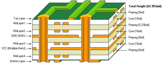
Via Technology in Multilayer PCBs: Through-Hole, Blind, and Buried Vias
Multilayer boards route signals up and down through the stack using three distinct via types, and each one trades off differently between cost, routing density, and manufacturing complexity.
Through-hole vias are the standard, lowest-cost option: a single drilled hole plated with copper that passes straight through every layer of the board. They're mechanically simple to produce and remain the default choice unless routing density forces a more specialized approach.
Blind vias connect an outer layer to one or more inner layers without drilling all the way through the board. Because they stop short of the opposite surface, they free up routing space on the layers they don't touch, which matters most in fine-pitch BGA and other high-density designs.
Buried vias connect two or more inner layers only, with no opening on either outer surface. They're drilled and plated before the remaining layers are laminated on top, which adds process steps compared to through-hole drilling.
Blind and buried vias show up mainly in HDI boards and multilayer designs of four layers or more, where a standard through-hole via would eat up routing space needed for dense component placement. They cost more than through-hole vias because of the added drilling and lamination steps, but they let designers pack more circuitry into the same board area without adding layers.
Multilayer PCB Advantages
Handles high complexity: routing space for dense, high-pin-count components.
Better signal integrity: dedicated ground and power planes reduce EMI and noise.
Smaller footprint, more functionality: layers stack vertically instead of spreading out.
Higher durability: extra layers add mechanical strength and aid heat dissipation.
Single connection point: replaces what might otherwise need several interconnected boards.
Multilayer PCB Disadvantages
Higher cost: more materials, precision fabrication, and skilled labor.
Longer lead times: lamination, alignment, and via drilling all add production time.
More complex design and manufacturing: requires specialized equipment and expertise.
Harder to repair: internal layers and buried vias aren't visible from the outside.
Common Multilayer PCB Applications
Multilayer boards are the standard in smartphones, laptops, servers and motherboards, medical imaging equipment (MRI, X-ray, CAT scan), automotive ECUs and infotainment systems, aerospace and military electronics, industrial control systems, and telecom infrastructure like base stations and satellite hardware.
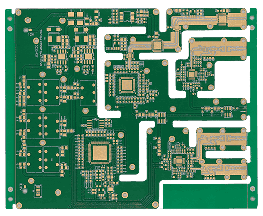
Single Layer vs Multilayer PCB: Side-by-Side Comparison
| Property | Single Layer PCB | Multilayer PCB |
|---|---|---|
| Conductive layers | 1 copper layer | 3 or more copper layers |
| Cost | Lowest manufacturing cost | Higher cost due to complex fabrication processes |
| Lead time | Shortest production time | Longer production time due to additional layers and processing steps |
| Design complexity | Simple designs with limited routing requirements | Complex and specialized designs for advanced electronics |
| Routing density | Low routing density | High routing density with more space for traces |
| Signal integrity | Basic signal performance without dedicated planes | Improved signal integrity with dedicated power and ground planes |
| Board size for equal function | Requires a larger board area to achieve the same functionality | Smaller and more compact for the same electrical functions |
| Repairability | Easier to inspect and repair | More difficult to troubleshoot and repair |
| Typical use case | Simple, single-function electronic devices | Complex, high-density electronic systems |
How to Decide: Single Layer or Multilayer PCB?
Run your project through these questions before committing to a stack-up:
How complex is the circuit? More traces than one plane can hold means more layers are needed.
What's the size constraint? Multilayer boards pack more function into less space.
Does the application demand high durability or harsh-environment tolerance?
What's the budget? A single-layer board is almost always cheaper if it can do the job.
How fast do you need the boards? Single-layer PCBs ship faster.
Does the circuit require high-speed or high-frequency performance?
There's also a middle ground worth knowing about: double-sided (double-layer) PCBs, which put copper on both sides of a single substrate — more routing room than single-layer boards, without the full cost of a true multilayer stack-up.
PCBgogo Provides High-Quality Solutions for Your Projects
PCBgogo supports single-layer through 40-layer PCB fabrication, covering both prototype runs and volume production, and offers PCB and PCBA as a one-stop service, from raw material sourcing through fabrication, assembly, and final inspection.
Material selection: Standard FR-4 across multiple TG grades (TG130-140, TG150-160, TG170-180) for stable thermal performance, plus advanced materials like Rogers and ceramic substrates for high-frequency or high-reliability designs.
Manufacturing process: Blind vias, buried vias, stacked vias, and laser drilling support high-density multilayer stack-ups, with tight control over board thickness tolerance, hole position, and controlled impedance. All boards are built to IPC-A-600 Class 2 as standard, with IPC-6012 Class 3 available on request.
AOI and X-ray inspection: Every board runs through automated optical inspection and X-ray inspection, catching solder joint and internal layer defects that aren't visible to the naked eye, before it ships.
Component assembly: Stable in-stock component inventory keeps common parts ready to go, backed by fully automated SMT lines that handle fine-pitch BGA and 0201 components daily, keeping PCBA quality consistent from placement through soldering.
After-sales service: Every order gets a free DFM review before production starts, and 24-hour customer service response.
Ready to build your board? Upload your Gerber files and get an instant PCB quote and see your project through from Gerber upload to finished board.
Conclusion
Neither single layer nor multilayer PCBs are universally "better" — they're built for different jobs. Single layer PCBs win on cost, simplicity, and speed for straightforward electronics. Multilayer PCBs win on density, performance, and durability for anything approaching modern consumer, medical, or industrial complexity. Matching the board to the actual requirements of the circuit is what keeps a project on budget and on schedule.
FAQ
Q: What is the main difference between a single layer PCB and a multilayer PCB?
A: A single-layer PCB has one conductive copper layer, while a multilayer PCB stacks three or more layers for greater routing capacity.
Q: Is a multilayer PCB always better than a single layer PCB?
A: No. Multilayer boards handle more complexity, but single-layer boards are cheaper, faster to make, and sufficient for simple circuits.
Q: How many layers does a smartphone PCB typically have?
A: Most smartphones use around 12 layers to fit dense, high-performance circuitry into a small space.
Q: Why are multilayer PCBs more expensive?
A: They require more materials, precise lamination, and specialized manufacturing equipment, which raises production cost.
Q: Can a single-layer PCB be repaired more easily than a multilayer PCB?
A: Yes. All traces are visible on one side, making faults easy to spot and fix compared to buried multilayer traces.
Q: What is a double-sided PCB, and how does it compare?
A: A double-sided PCB has copper on both sides of one substrate, offering more routing room than single layer boards at a lower cost than true multilayer designs.
Q: Which PCB type is best for high-speed or high-frequency circuits?
A: Multilayer PCBs are better suited, since dedicated ground and power planes improve signal integrity.
Q: Do single-layer PCBs limit board size?
A: Yes. Because everything must fit on one plane, boards often need to be larger to accommodate the same functionality a multilayer board could fit in less space.





