
 日本語
日本語
 한국어
한국어

RF Microwave PCB: Complete Design and Material Selection Guide
A single impedance mismatch along a 50 ohm microstrip trace can degrade a 28 GHz 5G signal by more than 3 dB before it ever reaches the antenna. That level of loss, invisible on a standard digital board, is what makes RF and microwave PCB design a fundamentally different discipline from conventional PCB engineering.
This guide covers material selection, stackup architecture, layout best practices, thermal management, and the key differences that separate high-frequency boards from standard PCBs.
What Is an RF/Microwave PCB?
An RF (radio frequency) or microwave PCB is a printed circuit board specifically designed to transmit high-frequency signals with minimal loss, reflection, and phase distortion. RF PCBs typically operate from about 100 MHz to several GHz, while microwave PCBs handle frequencies from roughly 2 GHz up to 77 GHz and beyond in millimeter wave applications.
At these frequencies, signals no longer behave as simple voltage differences between two points. They propagate as electromagnetic waves along transmission line structures, where every trace becomes a distributed circuit element. Inductance, capacitance, and resistance vary continuously along the signal path. A 1 mm stub that would be electrically invisible at 10 MHz can become a resonant antenna at 10 GHz, radiating energy and corrupting the signal entirely.
This is why standard FR4 boards fail at microwave frequencies: the substrate's dielectric constant (Dk) varies too much with frequency and temperature, and its dissipation factor (Df) turns too much signal energy into heat. According to Rogers Corporation's published material datasheets, FR4 typically exhibits a Df of 0.015 to 0.020 at 10 GHz, while a microwave-grade laminate like RO4350B maintains a Df of just 0.0037 at the same frequency, representing nearly an 80% reduction in signal loss per unit length.
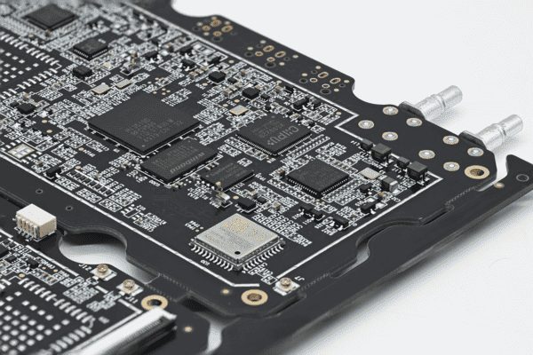
Key Differences Between RF, Microwave, and Standard PCBs
Standard PCBs, RF PCBs, and microwave PCBs differ across six critical dimensions: frequency range, signal behavior, substrate materials, design complexity, impedance tolerance, and manufacturing precision. The table below summarizes how each board type addresses these parameters.
| Parameter | Standard PCB | RF PCB | Microwave PCB |
|---|---|---|---|
| Frequency Range | DC to ~100 MHz | 100 MHz to ~2 GHz | 2 GHz to 77+ GHz |
| Signal Behavior | Simple voltage connections | Transmission line propagation | Electromagnetic wave propagation with precise field control |
| Typical Substrate | FR4 (Dk ~4.2 to 4.6) | Improved FR4 or Rogers 4000 series | PTFE, ceramic filled PTFE, advanced laminates |
| Impedance Tolerance | ±15 to 20% | ±5 to 10% | ±2 to 5% |
| Dissipation Factor (Df) | 0.015 to 0.025 | 0.003 to 0.008 | 0.0009 to 0.004 |
| Typical Applications | Computers, power supplies, digital logic | WiFi, Bluetooth, GPS, LTE | Radar, satellite, 5G mmWave, aerospace telemetry |
The Df values in the table above come from published manufacturer datasheets for standard FR4 (Shengyi S1141), Rogers RO4350B, and Rogers RT/duroid 5880, respectively. The key takeaway is that moving from standard to microwave-grade materials reduces signal loss by 80 to 95 percent, which becomes non-negotiable above 2 GHz.
Material Selection for High Frequency PCBs
Substrate material is the single most consequential choice in RF and microwave PCB design. Two material properties dominate the decision: dielectric constant (Dk), which determines the signal propagation speed and trace dimensions for a given impedance, and dissipation factor (Df), which controls how much signal energy converts to heat. Low Df means less insertion loss. A stable Dk across temperature and frequency means predictable impedance.
The table below compares the major high-frequency laminate families across five parameters that drive real design decisions.
| Material Series | Type | Dk (10 GHz) | Df (10 GHz) | Best For | Relative Cost |
|---|---|---|---|---|---|
| Rogers RO4350B | Hydrocarbon ceramic | 3.48 | 0.0037 | General RF, under 20 GHz | Moderate |
| Rogers RO4003C | Hydrocarbon ceramic | 3.38 | 0.0027 | Low loss RF, patch antennas | Moderate |
| Rogers RT/duroid 5880 | PTFE glass microfiber | 2.20 | 0.0009 | Ultra low loss, mmWave, 77 GHz radar | High |
| Rogers RO3003 | PTFE ceramic | 3.00 | 0.0010 | Stable to 77 GHz, automotive radar | High |
| Panasonic Megtron 6 | Low Dk glass/epoxy | 3.61 | 0.0040 | High speed digital + RF hybrid, HDI | Moderate |
| Taconic TLY-5 | PTFE woven glass | 2.20 | 0.0009 | Low loss mmWave, satellite comms | High |
| Isola Tachyon-100G | Very low loss thermoset | 3.00 | 0.0021 | 100 Gbps digital and microwave hybrid | High |
When cost is a primary constraint, hybrid stackups combining a thin layer of RF laminate on the outer layers with standard FR4 cores offer a practical middle ground. This approach preserves high frequency performance on critical signal layers while reducing total board cost by 40 to 60 percent compared to an all PTFE construction, according to industry fabrication cost models published by Epec and other PCB manufacturers.
Stackup Design for RF and Microwave Boards
RF and microwave PCB stackup design establishes the physical arrangement of signal, ground, and dielectric layers to create stable transmission line environments. A properly designed stackup ensures that every RF trace sees a consistent impedance, typically 50 ohms for microstrip lines, with an uninterrupted return path directly beneath it.
The fundamental rule is that every RF signal layer must be adjacent to a solid, continuous ground plane. This pairing forms the transmission line structure: in a microstrip configuration, the signal trace sits on the top layer with the ground plane directly below, separated by a dielectric of known thickness and Dk. For a four-layer board, the most common RF stackup places RF signals on layer 1, a solid ground on layer 2, power and digital signals on layer 3, and a second ground on layer 4. The distance between layer 1 and layer 2 directly determines the trace width needed to achieve 50 ohms.
For a 50 ohm microstrip on Rogers RO4350B (Dk 3.48) with 0.5 oz copper and a 0.254 mm dielectric thickness, the required trace width is approximately 0.55 mm. Reducing the dielectric thickness to 0.127 mm shrinks the required trace width to about 0.27 mm. These calculations follow the IPC 2141 standard microstrip impedance formula, which is accurate to within 2 percent for traces wider than the dielectric height. Hybrid multilayer constructions, where PTFE or ceramic-filled laminates form the outer RF layers and FR4 cores handle inner power and digital routing, have become the industry standard approach for balancing performance and cost.
Applications of RF and Microwave PCBs
RF and microwave PCBs appear in every system that transmits or receives wireless signals above 100 MHz. The specific application determines which frequency band, power level, and board material is most appropriate. Here are the major application categories and what drives their PCB requirements:
5G base stations and mmWave small cells: Operating at 24 GHz to 39 GHz, these systems demand ultra-low-loss materials like Rogers RO3003 or RT/duroid 5880 with Df values below 0.002. Phase stability across temperature is critical for beamforming arrays, where inconsistent phase shift between antenna elements degrades the beam pattern. A typical 64-element phased array at 28 GHz requires impedance matching to within ±2 ohms across every channel.
Automotive radar at 24 GHz and 77 GHz: Adaptive cruise control, blind spot detection, and automated emergency braking all rely on microwave radar modules built on PTFE-based laminates. The 77 GHz band demands materials with Dk tolerance within ±0.05 and extremely smooth copper profiles to minimize conductor loss at these short wavelengths. Rogers RO3003 and Taconic TLY series dominate this application segment.
Satellite communication terminals: VSAT terminals, satellite TV receivers, and phased array user terminals operate across Ku band (12 to 18 GHz) and Ka band (26.5 to 40 GHz). These boards must handle both high-frequency RX/TX signals and DC power distribution for LNB and BUC components, often requiring hybrid multilayer constructions with heavy copper inner layers for power handling.
Aerospace and defense electronic warfare systems: Jamming systems, radar warning receivers, and secure communication links push frequency limits into the millimeter wave range. These boards must also meet MIL spec requirements for thermal cycling, vibration, and outgassing. RT/duroid 6002 with its copper-matched coefficient of thermal expansion addresses the mechanical reliability challenges of these demanding environments.
Medical imaging and telemetry: MRI systems use RF power amplifiers and receiver coils operating at Larmor frequencies (typically 64 MHz for 1.5T and 128 MHz for 3T scanners). The PCB inside an MRI RF coil must maintain precise impedance matching to the coil element while withstanding high peak RF power. Medical telemetry devices operating in the 2.4 GHz ISM band use compact multilayer RF boards with integrated antennas.
Test and measurement equipment: Vector network analyzers, spectrum analyzers, and signal generators contain precision RF boards that must maintain flat frequency response and low phase noise across multi-octave bandwidths. These applications often use thick, low Dk materials like RT/duroid 5880 to achieve wider trace geometries that reduce conductor loss at very high frequencies.
Across all these applications, the common thread is that the PCB is not just an interconnection platform. It is an active part of the RF signal chain, and its material choices, trace geometries, and grounding architecture directly determine the system's noise figure, gain flatness, and phase linearity.
RF PCB Layout Best Practices
RF and microwave PCB layout requires a different set of priorities than digital PCB design. Signal integrity is not a secondary concern. It is the primary constraint that drives every placement and routing decision. The following practices encapsulate what experienced RF designers apply across every board:
Controlled impedance on every RF trace: Every RF signal path must be designed as a transmission line with a target characteristic impedance, typically 50 ohms for most systems. Trace width, dielectric thickness, and copper weight are calculated together using the IPC 2141 microstrip or stripline formulas. A 10 percent deviation from target impedance causes a return loss of roughly 20 dB, which may be acceptable for some applications, but a 20 percent deviation drops return loss to about 14 dB and becomes problematic for sensitive receiver front ends.
Uninterrupted ground plane directly beneath every RF trace: The return current at high frequencies follows the path of least inductance, not the path of least resistance. That path is directly under the signal trace in the reference plane. Any gap, slot, or split in the ground plane beneath an RF trace forces the return current to detour, creating a loop antenna that radiates and a series impedance discontinuity that reflects signal energy. On a 10 GHz microstrip, a 2 mm ground gap can cause a 1 dB insertion loss penalty.
No sharp bends in RF routing: A 90-degree corner on a microstrip line creates a local impedance discontinuity because the effective trace width changes at the apex. The industry standard replacement is a mitered bend (two 45 degree segments) or a swept radius curve with a bend radius at least three times the trace width. For a 50 ohm line at 10 GHz, this means a minimum bend radius of approximately 1.5 mm to 2 mm.
Via stitching along ground plane edges and RF trace perimeters: Ground vias spaced at intervals of one tenth wavelength or less create a low impedance fence that suppresses parallel plate modes and reduces edge radiation. At 30 GHz, this means ground via spacing no more than 0.5 mm along the perimeter of each RF section. Via stitching also reduces coupling between adjacent RF channels, improving isolation by 10 to 20 dB compared to unstitched layouts.
Physical separation of RF, digital, and power sections: Digital switching noise from microcontrollers, FPGAs, or DC-DC converters can couple into sensitive RF receiver stages through the substrate, power planes, or radiated fields. A minimum spacing of 5 mm between RF and noisy digital sections, combined with separate power distribution and ground pour partitioning, provides meaningful isolation. For the most sensitive LNAs and VCOs, a grounded metal shield may be necessary.
Minimize via count on RF signal paths: Each via adds roughly 0.5 nH to 1 nH of series inductance and creates a small impedance discontinuity. At 10 GHz, a single via with 1 nH of inductance presents a reactance of about 63 ohms, enough to measurably degrade return loss. When layer transitions are unavoidable for dense routing, backdrilling to remove the unused via stub prevents that stub from becoming a quarter-wave resonator.
These practices are not independent. Impedance control depends on the ground plane, which depends on via stitching, which depends on routing discipline. They form an interdependent system where any single weak link degrades overall RF performance.
Thermal Management in High Frequency PCBs
Thermal management in RF and microwave PCBs addresses the challenge that many high-performance RF laminates conduct heat significantly less effectively than standard FR4, while the components mounted on them (power amplifiers, GaN transistors, and high-speed converters) generate substantial heat in concentrated areas.
The thermal conductivity of standard FR4 is approximately 0.3 to 0.4 W/m/K. Rogers RO4350B is similar at 0.6 W/m/K, and RT/duroid 5880 is even lower at about 0.2 W/m/K. In contrast, a thermally optimized RF material like Rogers RT/duroid 6035HTC achieves 1.44 W/m/K, nearly a fivefold improvement over standard PTFE laminates. This matters because a GaN power amplifier dissipating 5 W into a 5 mm by 5 mm package footprint creates a heat flux density of 200,000 W/m2. Without an effective thermal path, the junction temperature rises beyond safe limits within seconds.
Thermal via arrays under high power components: A dense grid of plated through-hole thermal vias directly beneath the component's thermal pad conducts heat vertically from the top layer to inner ground planes and the bottom side. Via density matters more than via diameter: a 3 by 3 grid of 0.3 mm vias on a 1 mm pitch lowers junction-to-case thermal resistance by roughly 30 to 50 percent in typical applications. Filling thermal vias with conductive epoxy or copper further improves heat transfer.
Ground planes as lateral heat spreaders: Heavy copper ground planes (1 oz or thicker) conduct heat laterally across the board, distributing it over a larger area where convection or conduction cooling can remove it more effectively. The thermal spreading resistance of a 1 oz copper plane is about 70 K/W per square, while a 2 oz plane halves this to roughly 35 K/W per square.
Metal core and metal backed PCB constructions: For the most thermally demanding applications, such as high power radar transmit modules, bonding the RF laminate directly to an aluminum or copper base plate provides a direct conductive path from the board to the system heat sink. Total thermal resistance from component junction to base plate can be below 1 K/W with a properly designed metal core stackup.
Component placement for thermal balance: High power amplifier chains should be placed with adequate spacing and staggered rather than lined up in a row, so that each device sees unimpeded airflow or conduction paths. Placing a low-noise amplifier immediately adjacent to a power amplifier creates a thermal gradient that degrades LNA noise figure by 0.5 to 1 dB simply through substrate heating.
The most effective thermal strategy combines multiple approaches: material selection for the application's power level, thermal via arrays sized to the specific component dissipation, adequate copper weight for spreading, and board-level placement that avoids hot spots. No single technique solves the thermal problem alone.
Common Problems and Solutions for RF and Microwave PCBs
RF and microwave PCB design presents a distinct set of recurring challenges. The table below pairs each common problem with its engineering solution, drawing on established industry practice and published application notes from Rogers Corporation and IPC guidelines.
| Problem | Solution |
|---|---|
| Impedance mismatch causing signal reflections | Calculate trace width against verified substrate Dk and thickness using IPC 2141 formulas. Specify impedance test coupons on the fabrication panel. Maintain ±5% impedance tolerance for RF and ±3% for microwave. |
| Excessive insertion loss at mmWave frequencies | Select ultra-low Df laminates (Df < 0.002) such as RT/duroid 5880 or TLY-5. Use wider traces where geometry permits. Specify low profile or rolled copper foil to reduce conductor surface roughness loss. |
| Ground plane discontinuities causing radiation and coupling | Never route RF traces across ground plane splits or gaps. Use continuous reference planes. Via stitch along section boundaries at λ/10 spacing. Run EM simulation (Ansys HFSS or Keysight ADS Momentum) to identify unexpected resonances. |
| Dielectric property variation with temperature shifting filter performance | Select materials with low thermal coefficient of Dk (TCDk), such as Rogers TMM series with TCDk below 20 ppm/°C. Validate design at temperature extremes through simulation before committing to fabrication. |
| Copper delamination or poor via plating in PTFE substrates | PTFE is chemically inert and resists electroless copper adhesion. Fabricators must use plasma etching or sodium naphthalene treatment before through-hole plating. Specify IPC 6012 Class 3 inspection criteria for plated holes. |
| Unwanted resonance from via stubs in thick multilayer boards | Backdrill via stubs to within 0.15 mm of the signal layer transition. At 28 GHz, a 0.5 mm stub length approaches quarter-wave resonance and can cause a deep notch in insertion loss. Backdrilling eliminates this stub. |
| Crosstalk between adjacent RF channels reduces isolation | Maintain center-to-center trace spacing of at least 3x the trace width for parallel runs. Insert ground guard traces with periodic via stitching between critical channels. For dense phased array feed networks, consider stripline over microstrip for superior isolation. |
| Thermal runaway in GaN power amplifier stages | Deploy thermal via arrays with conductive fill under the device thermal slug. Use high thermal conductivity laminates (RT/duroid 6035HTC or Rogers TC350). Monitor board temperature at the package base during prototype characterization. |
Future Trends in RF and Microwave PCB Technology
The RF and microwave PCB industry is being reshaped by three converging forces: the push to millimeter wave and sub-terahertz frequencies for 6G and sensing, the demand for smaller and more integrated RF front ends, and the need for materials that simultaneously deliver low loss and high thermal performance. Here are the trends that will define the next five years:
Millimeter wave and D band (110 to 170 GHz) expansion: 6G research and high-resolution imaging are pushing operating frequencies beyond 100 GHz, where trace dimensions shrink to sub-millimeter scales and copper surface roughness becomes a dominant loss mechanism. Materials like Rogers RO3003G2 and Isola Tachyon-100G, with Df values at or below 0.001 at 100 GHz, are being qualified for these bands. Fabrication tolerances tighten to ±0.025 mm for critical features.
Antenna in package (AiP) and system in package (SiP) integration: Rather than placing the antenna on the PCB and connecting it through a separate RF connector, AiP integrates the antenna array directly into the IC package substrate. This reduces interconnect loss by 1 to 2 dB at 28 GHz and shrinks the overall module footprint. The PCB's role shifts from antenna carrier to baseband and power management, though it still requires controlled impedance routing up to the package interface.
Ultra-low-loss thermoset materials replacing PTFE in volume applications: PTFE remains the gold standard for loss performance, but its high fabrication cost and cold flow properties make it difficult to process. Newer thermoset materials like Rogers RO4835 and Isola TerraGreen achieve Df values approaching 0.002 with FR4-compatible processing, enabling lower-cost multilayer RF boards for automotive and 5G CPE applications.
Additive manufacturing and 3D printed RF structures: Selective laser sintering of conductive and dielectric pastes enables true 3D RF structures: non-planar antennas, conformal arrays, and waveguide filters printed directly onto curved surfaces. While still in early commercialization, additive RF manufacturing could eliminate the planar constraint that has defined PCB-based microwave design for decades.
AI-assisted RF layout automation: Machine learning models trained on thousands of EM simulation results are beginning to automate portions of RF layout, such as via placement optimization and impedance discontinuity correction. These tools do not replace skilled RF designers, but they accelerate the iterative simulation and refinement cycle that dominates microwave board development timelines.
Each of these trends points toward tighter integration, higher frequencies, and greater reliance on simulation and automation in the design workflow. The fundamental physics of transmission line behavior will not change, but the tools, materials, and architectures available to manage it will continue to advance rapidly.
Frequently Asked Questions About RF and Microwave PCBs
What is the difference between an RF PCB and a microwave PCB?
RF PCBs typically operate from about 100 MHz to 2 GHz, while microwave PCBs handle frequencies from 2 GHz up to 77 GHz and beyond. The distinction matters because signal behavior changes: above roughly 2 GHz, distributed effects dominate and every interconnect feature must be modeled as a transmission line element rather than a lumped component.
Can FR4 be used for RF PCB designs?
FR4 is generally unsuitable above 500 MHz due to its high and unstable dissipation factor (Df 0.015 to 0.020) and wide Dk variation with temperature and frequency. For low-cost applications below 1 GHz with relaxed performance requirements, some improved FR4 variants with lower Df may be acceptable. Above 1 GHz, switching to a purpose-built RF laminate provides measurable insertion loss improvement.
Why is 50 ohms the standard impedance for RF PCBs?
The 50 ohm standard emerged as a compromise between maximum power handling (which peaks at 30 ohms for coaxial structures) and minimum loss (which bottoms at 77 ohms for air dielectric). The IEEE and IPC adopted 50 ohms as the industry standard, and the entire RF test and measurement ecosystem (VNA ports, cables, connectors) is built around this value, making it the practical default for most designs.
How do I choose between microstrip and stripline for RF routing?
Microstrip (signal on an outer layer above a ground plane) is simpler to fabricate, provides easier access for tuning, and uses fewer layers. Stripline (signal buried between two ground planes) offers superior isolation and lower radiation loss but requires at least three layers and presents tighter trace width constraints. Choose microstrip for most general RF designs below 10 GHz where cost and accessibility matter. Choose stripline for dense, high isolation designs or where EMI containment is critical.
What surface finish should I use for RF and microwave PCBs?
ENIG (electroless nickel immersion gold) is the most common finish for RF boards because it provides a flat, solderable surface with good shelf life. However, the nickel layer adds resistance and can increase insertion loss at very high frequencies. For mmWave designs above 30 GHz, immersion silver or ENEPIG (electroless nickel, electroless palladium, immersion gold) offer lower-loss alternatives. Bare copper with OSP is the lowest loss option but has limited shelf life.
How do I verify impedance control in a fabricated RF PCB?
Most fabricators include impedance test coupons on the same panel as the production boards. These coupons replicate the target trace geometry and are measured with a TDR (time domain reflectometer) to verify impedance. For production qualification, specify that coupons be measured and reported, and set a tolerance (typically ±10% for RF, ±5% for microwave) with the fabricator before releasing the design.
Conclusion
RF and microwave PCB design succeeds or fails on the fundamentals: choosing the right substrate for the frequency and power level, designing a stackup that creates stable transmission line environments, and executing a layout where every trace, via, and ground pour serves the signal integrity requirements of the application. There are no shortcuts in high frequency design, but the discipline of following established best practices produces boards that perform predictably from the first prototype.
Whether you are designing a 2.4 GHz WiFi front end on RO4350B or a 77 GHz automotive radar on RO3003, start with the substrate datasheet, calculate your transmission line dimensions, maintain continuous reference planes, and simulate critical sections before committing to fabrication. The materials and tools available to RF designers today are more capable than ever, and a methodical approach to the fundamentals will consistently deliver results.





