




 日本語
日本語
 한국어
한국어

PCB X-Ray Inspection: Process, Defects & Standards
Many of the most serious PCB assembly defects are impossible to see from the surface. Solder joints beneath BGAs, QFNs, LGAs, and other bottom-terminated components remain hidden after reflow, even when the board looks perfect under a microscope.
PCB X-ray inspection solves this problem by examining solder joints and internal structures without cutting or damaging the board. It can reveal solder voids, hidden bridges, insufficient solder, component misalignment, poor plated-through-hole fill, and other defects that visual inspection or AOI may miss.
This guide explains how PCB X-ray inspection works, what it can and cannot detect, when it should be specified, and how to define meaningful inspection requirements for your PCB assembly project.
What Is PCB X-Ray Inspection?
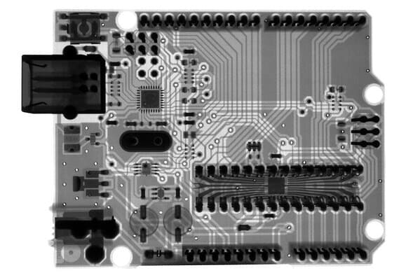
PCB X-ray inspection is a non-destructive inspection method that uses X-rays to examine structures hidden beneath components or inside a printed circuit board assembly.
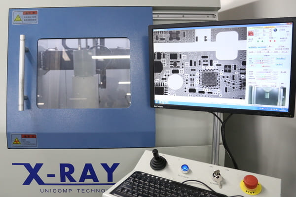
An X-ray system directs controlled radiation through the PCBA and records the transmitted energy with a detector. Materials with different thicknesses and densities attenuate X-rays differently, producing a grayscale image of solder, copper, component structures, vias, and substrate materials.
Depending on how the equipment displays the image, high-attenuation materials such as solder may appear lighter or darker. Therefore, an inspector should interpret relative contrast, geometry, and consistency rather than relying on color alone.
X-ray inspection is primarily used during PCB assembly, although it can also support bare PCB analysis in areas such as:
Multilayer registration
Drilled-hole alignment
Via and barrel analysis
Internal copper feature verification
Failure analysis of buried structures
When the system automatically captures and evaluates images against programmed criteria, the process is called Automated X-ray Inspection, or AXI.
Why Is X-Ray Inspection Important for Modern PCB Assemblies?
AOI and visual inspection depend on a clear line of sight. They work well for component presence, polarity, placement, and visible solder fillets, but they cannot directly inspect joints underneath an opaque component body.
This becomes a major limitation when a design includes:
Ball Grid Arrays (BGAs)
Micro-BGAs
Quad Flat No-Lead packages (QFNs)
Land Grid Arrays (LGAs)
Chip Scale Packages (CSPs)
Bottom-terminated power components
Large exposed thermal pads
Shielded or densely populated areas
A BGA may contain hundreds of connections beneath a single package. One hidden bridge, open joint, or non-wetted solder ball can cause intermittent operation or complete board failure.
X-ray inspection reduces this blind spot. It also provides process engineers with information that can be used to improve stencil apertures, solder paste deposition, placement accuracy, reflow profiles, and component handling.
How Does PCB X-Ray Inspection Work?
A typical PCB X-ray inspection process includes four main elements:
An X-ray source generates controlled radiation.
The PCB assembly is positioned between the source and detector.
X-rays pass through the assembly and are attenuated by different materials.
Software converts the detector data into an image for manual or automated analysis.
The inspector then evaluates features such as solder-joint shape, ball diameter, spacing, alignment, solder distribution, and void area.
Magnification can often be increased by moving the board closer to the X-ray source. However, usable image quality depends on more than magnification. Focal spot size, detector resolution, board thickness, material density, imaging angle, and software processing all affect what the system can resolve.

2D vs. 2.5D vs. 3D PCB X-Ray Inspection
Not every assembly needs the most advanced X-ray method. The correct choice depends on component geometry, board density, production volume, and the purpose of the inspection.
| Inspection method | How it works | Best suited for | Main limitation |
|---|---|---|---|
| 2D X-ray | Produces a projection through the complete assembly | Routine BGA inspection, bridges, large voids, alignment and solder distribution | Features on opposite sides may overlap |
| 2.5D X-ray | Captures angled or oblique views | Double-sided assemblies and joints obscured in a top-down image | Does not provide a complete volumetric model |
| 3D X-ray / CT | Reconstructs multiple projections into cross-sectional slices | Complex failure analysis, overlapping structures and advanced packages | Slower and more expensive |
| Inline AXI | Automatically inspects programmed locations during production | Repeatable, higher-volume inspection | Requires programming, validation and process-specific limits |
For many prototype and standard BGA assemblies, 2D X-ray provides sufficient information. A double-sided board with overlapping components may require angled imaging or CT to separate the features.
3D X-ray is not automatically better for every project. It should be selected when the additional depth information materially improves defect detection or root-cause analysis.
What Defects Can PCB X-Ray Inspection Detect?
1. BGA solder voids
Voids are gas pockets or unfilled areas inside a solder joint. X-ray inspection can measure their projected area and show whether they are isolated, clustered, or repeated across multiple solder balls.
A common measurement is: Void percentage = projected void area / projected solder-joint area x 100%.
The percentage alone does not tell the full story. Void location, distribution, joint geometry, package type, thermal requirements, and product reliability class must also be considered.
2. Hidden solder bridges
A solder bridge connects adjacent terminals that should remain electrically isolated. Under a BGA or LGA, the bridge cannot be seen by AOI.
In an X-ray image, the inspector looks for abnormal material connecting adjacent balls or lands. Electrical testing should still be used to confirm whether a short circuit exists.
3. Insufficient or excessive solder
Variations in solder volume can change a joint's apparent size, density, or shape. Insufficient solder can reduce mechanical strength or create an open connection, while excessive solder may increase the risk of bridging.
If the same pattern appears across several components, the X-ray result can indicate a stencil, printing, paste-release, or placement problem.
4. BGA misalignment
A correctly assembled BGA normally shows a regular array with consistent spacing and joint shape. Offset rows, uneven collapse, or compressed joints on one side may indicate placement error, package movement, or uneven reflow.
5. Head-on-pillow and non-wet opens
A head-on-pillow defect occurs when a BGA ball and solder paste reflow but fail to form one complete metallurgical joint. Component warpage, oxidation, and insufficient flux activity are possible causes.
Some head-on-pillow defects produce a recognizable separation or unusual joint profile. However, routine 2D X-ray does not detect every case reliably. Angled imaging, CT, electrical testing, dye-and-pull testing, or cross-section analysis may be required when the result is uncertain.
6. QFN thermal-pad voiding
The exposed pad beneath a QFN is often used for heat transfer and grounding. X-ray inspection can show solder coverage and void distribution across this hidden pad.
Large or strategically located voids may reduce the effective thermal path. The acceptable result should be defined using component requirements, product reliability targets, assembly drawings, and customer-supplier agreement rather than an assumed universal percentage.
7. Plated-through-hole solder fill
X-ray inspection can help assess solder distribution in plated-through holes when the condition cannot be fully observed from the exterior. Oblique imaging is often more useful than a single top-down projection because it provides information along the barrel height.
8. Internal PCB registration issues
During bare PCB or failure analysis, X-ray can help identify drilled-hole offset, annular-ring concerns, internal layer misregistration, and some via-related abnormalities.
X-ray should not be treated as a replacement for inner-layer AOI, electrical testing, microsection analysis, or other fabrication controls.
AOI vs. X-Ray vs. ICT vs. Functional Testing
| Method | What it evaluates | Best applications | Important limitation |
|---|---|---|---|
| Visual inspection | Surface appearance | Obvious damage, workmanship and manual checks | Operator-dependent; cannot see hidden joints |
| AOI | Visible components and solder features | Missing parts, polarity, placement, visible bridges and fillets | Cannot inspect beneath opaque packages |
| X-ray / AXI | Hidden physical structures | BGA, QFN, LGA, voids, hidden bridges and solder distribution | Does not prove electrical functionality |
| ICT | Circuit-level electrical characteristics | Shorts, opens, resistance, capacitance and component presence | Requires test access and often a fixture |
| Flying probe | Electrical connectivity without a dedicated fixture | Prototypes and lower-volume production | Slower than fixture-based ICT |
| Functional testing | Operation of the completed assembly | Interfaces, power, firmware and real functions | May not reveal the physical cause of a failure |
These methods are complementary. A robust PCBA quality plan may use SPI before placement, AOI after placement or reflow, X-ray for hidden joints, and electrical or functional testing before shipment.
Does Every PCB Assembly Need X-Ray Inspection?
No. Applying X-ray to every board and every component can add cost and inspection time without necessarily improving quality.
X-ray inspection is usually recommended when one or more of the following conditions apply:
The assembly contains BGA, LGA, CSP or bottom-terminated packages.
A QFN or power device relies on a large exposed thermal pad.
The board uses fine-pitch or high-density assembly.
Critical solder joints cannot be inspected optically.
The product will experience significant thermal cycling or vibration.
A first article must be verified before production.
The project has automotive, aerospace, medical, industrial or other high-reliability requirements.
An electrical failure requires physical root-cause analysis.
The customer requires X-ray records or traceability.
A simple assembly containing visible gull-wing leads, chip resistors, capacitors and through-hole connectors may be adequately covered by AOI, visual inspection and electrical testing.
A more useful question than 'Does this PCB need X-ray?' is: Which defects present the greatest risk in this design, and which inspection method can actually detect them?
PCB X-Ray Inspection Workflow
1. Review the assembly design
The manufacturer identifies hidden-joint packages, critical components, double-sided overlap, thermal pads and high-reliability areas.
2. Define the inspection scope
The customer and manufacturer agree on components to inspect, sampling or 100% inspection, imaging method, product class, acceptance criteria, reporting format and disposition of marginal results.
3. Create or select an inspection program
For AXI, component coordinates and expected joint geometry may be generated from CAD, Gerber, centroid, BOM and package data.
4. Capture and evaluate images
The system or operator evaluates the specified joints. Automated results should be reviewed when an image is ambiguous or the equipment flags a borderline condition.
5. Classify and contain defects
Suspect boards are separated from accepted assemblies. The manufacturer determines whether the defect is isolated or represents a broader process trend.
6. Correct the root cause
The investigation may lead to adjustments in stencil aperture design, solder paste volume, paste handling, placement pressure, component storage, reflow profile, pad geometry or via-in-pad design.
7. Verify rework or process changes
Reworked assemblies and subsequent production should be reinspected to confirm that the corrective action was effective.
IPC Standards and X-Ray Acceptance Criteria
PCB X-ray inspection should be tied to the correct product requirements. Relevant documents include:
IPC-A-610J, which provides post-assembly acceptability criteria.
J-STD-001J, which establishes requirements for soldered electrical and electronic assemblies.
IPC-7095E, which provides design and assembly process guidance for BGA and fine-pitch BGA technology.
IPC released the J revisions of IPC-A-610 and J-STD-001 in 2024, while IPC-7095E was published in August 2024. IPC also states that IPC-7095 provides process guidance, while contractual BGA accept/reject requirements are established through J-STD-001 and IPC-A-610. Check the IPC document revision table and the IPC-7095E overview when defining current project requirements.
There is no single void percentage that can be safely applied to every BGA, QFN, thermal pad, solder alloy and product class. The applicable standard revision, component type, customer drawing and contractual agreement must be identified first.
For critical projects, define the following before production:
Standard and revision
IPC product class
Package-specific requirements
Individual and cumulative void measurement rules
Whether projected area or another method is used
Sampling level
Image retention period
Rework and concession procedure
How to Choose a PCB Assembly Manufacturer with X-Ray Capability
Owning an X-ray machine is only one part of an effective inspection process. Before placing an order, ask the manufacturer:
Which components are inspected by default?
Is the inspection manual, automated, inline or offline?
Is 2D, angled, 2.5D or 3D imaging available?
Can the system inspect double-sided assemblies without confusing overlapping features?
Is inspection performed on a sample or every critical component?
Which IPC standard and revision are used?
Can the manufacturer measure and report void area?
Are X-ray images available with the inspection report?
How are marginal results reviewed?
How are defects connected to corrective action and process improvement?
PCBgogo uses X-ray and AOI equipment as part of its PCB assembly inspection capabilities, including inspection for complex assemblies such as those containing BGAs. The PCBgogo PCB assembly quotation page also allows customers to select X-ray testing when submitting a project.
For controlled projects, include the components, inspection scope, sampling requirement, acceptance standard and reporting format in your RFQ or assembly notes.
PCBgogo - Reliable, High-Quality PCB Manufacturing
Save time and money with an all-in-one solution for PCB fabrication, assembly, and parts. Reduce vendor coordination, avoid split shipments, and get consistent, reliable quality.
Get Free Quote >
Frequently Asked Questions
Can X-ray inspection detect all BGA defects?
No. It is effective for voids, bridges, solder distribution, alignment and some open-joint conditions, but certain head-on-pillow defects, cracks or metallurgical problems may require CT, electrical testing or destructive analysis.
Can X-ray inspection replace AOI?
No. AOI is faster and better suited to visible placement, polarity and solder defects. X-ray is used for hidden structures. Many assembly lines use both.
Can X-ray inspection replace functional testing?
No. X-ray evaluates physical structures but does not confirm firmware, component values, electrical performance or complete product operation.
Is 3D X-ray always better than 2D X-ray?
No. Standard 2D imaging is often sufficient for routine BGA and QFN inspection. 3D CT is most valuable when structures overlap, or detailed cross-sectional information is required.
Does X-ray inspection damage electronic components?
Industrial PCB X-ray inspection is designed as a non-destructive process. However, dose sensitivity and cumulative exposure should be evaluated for radiation-sensitive components or unusual inspection conditions.
Should X-ray inspection be requested before production?
Yes. Early agreement allows the manufacturer to define the inspection locations, equipment, sampling plan, acceptance criteria, and report format before assembly begins.
Is X-ray inspection used for bare PCBs or only PCBAs?
It is most commonly used for PCB assemblies, but it can also support inspection of multilayer registration, drilled-hole alignment, internal copper structures and certain via defects.
Conclusion
PCB X-ray inspection closes an important quality-control gap by revealing solder joints and internal features that AOI cannot see. It is particularly valuable for BGAs, QFNs, LGAs, CSPs, exposed thermal pads and complex double-sided assemblies.
The best inspection plan is not simply the one using the most advanced equipment. It is the one that matches the assembly's actual risks, uses clearly defined acceptance criteria, and combines X-ray results with optical, electrical and functional testing.
If your design contains hidden solder joints, submit your Gerber files, BOM, centroid data and inspection requirements through the PCBgogo PCB assembly quote page. Specify X-ray testing and any required reporting criteria so the engineering team can review the assembly before production.





