



 日本語
日本語
 한국어
한국어

PCB Soldering: 4 Methods and How to Choose the Right One
QUICK ANSWER PCB soldering is the process of forming electrical and mechanical bonds between component leads and PCB pads using a molten metal alloy. In production, it is not a single technique — it includes hand soldering, wave soldering, reflow soldering, and selective soldering, each suited to different component types, production volumes, and cost targets. Choosing the right method, alloy, and joint standard early is critical to ensuring the board passes inspection and performs reliably in real-world use.
Years of pulling boards off assembly lines have taught me one thing: the solder joints that cause the most trouble are never the ones you can see. A cold joint at least shows up dull and grainy under AOI. A void trapped under a BGA doesn't show up at all, not until someone runs an X-ray, or worse, not until the board fails in the field six months later.
Heat, melt, inspect gets you through a hand-soldered prototype just fine. It stops covering the real decisions the moment a board needs reflow for a QFN, a joint class specified before final QC, or a stencil aperture sized correctly before paste ever touches the pad. Those calls get made weeks before anyone picks up an iron, and getting them wrong is usually what turns into a rejected board later.
This guide walks through how a solder joint actually forms and compares the four soldering methods used in PCB assembly, so you can match the right method, alloy, and joint class to your board before it goes into production, not after a defect shows up.
How a Solder Joint Actually Forms
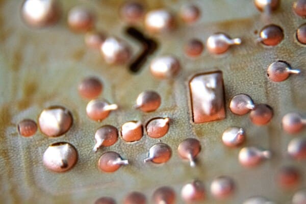
Every solder joint, regardless of method, goes through the same underlying metallurgical sequence. A flux — a mildly acidic chemical agent — first strips oxidation from the copper pad and component lead so the base metals are chemically clean. As the solder alloy melts, it wets the exposed copper and begins diffusing into it, forming a thin intermetallic compound (IMC) layer at the interface. This IMC layer is what actually creates the bond; it is not glue holding two surfaces together, but a genuine metallurgical alloy formed between the solder and the copper. When the joint cools, the solder solidifies around that IMC layer, locking the mechanical and electrical connection in place.
The alloy used for that molten metal has shifted significantly over the past two decades because of RoHS restrictions on lead. The table below compares the two dominant families in use today.
| Property | Sn63/Pb37 (Leaded) | SAC305 (Lead-Free, Sn/Ag/Cu) |
|---|---|---|
| Melting point | ~183°C, eutectic | ~217–221°C |
| Wetting behavior | Fast, forgiving | Slower, more sensitive to flux and cleanliness |
| Joint appearance | Bright, smooth | Slightly duller, more granular finish |
| Regulatory status | Restricted under RoHS for most consumer goods | RoHS-compliant, required for CE-marked consumer electronics |
| Typical use case | Aerospace, military, medical (RoHS-exempt classes) | Consumer, industrial, automotive electronics |
The higher process temperature of SAC305 matters beyond the solder itself — it raises the thermal stress placed on components, the PCB substrate, and the solder mask during reflow, which is one reason thermal profile design gets more attention on lead-free boards than it used to on leaded ones.
The Four PCB Soldering Methods
Almost all production soldering falls into one of four categories. Each exists because no single method is efficient across every component type and volume.
1. Hand (Manual) Soldering
A technician applies a heated iron and solder wire joint-by-joint. This remains the standard for prototypes, low-volume runs, through-hole rework, and fixing defects flagged after automated inspection. It's the most flexible method and requires no tooling investment, but throughput is limited by operator speed and joint quality varies with skill level.
2. Wave Soldering
The populated board passes over a standing wave of molten solder, which contacts the underside of the board and solders all exposed through-hole leads simultaneously. Wave soldering is efficient for boards that are through-hole dominant or mixed-technology boards where SMT components are wave-compatible or protected. It scales well for volume but is largely unsuitable for fine-pitch SMT, since exposing the top-side SMT paste to a solder wave risks bridging and component shift.
3. Reflow Soldering
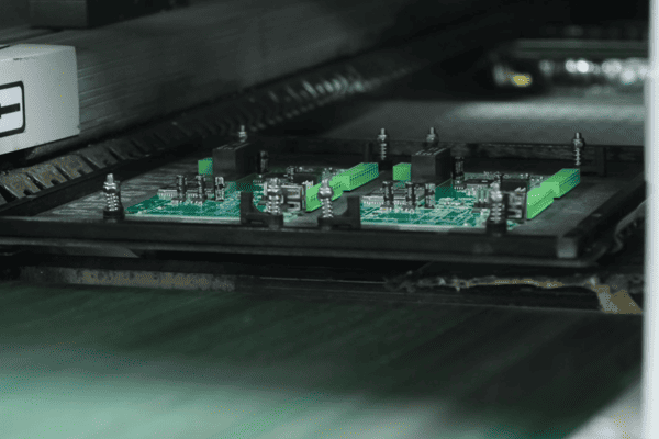
Solder paste — a suspension of tiny solder particles in flux — is printed onto pads through a stencil, components are placed into the wet paste, and the board travels through a reflow oven with a controlled multi-zone thermal profile: preheat, soak, reflow, and cooling. This is the standard method for SMT assembly and the only practical way to solder fine-pitch and area-array packages such as BGA, QFN, and LGA, where leads or terminations sit underneath the component body and are inaccessible to a hand iron.
Profile accuracy matters more here than in any other method. Too fast a ramp during preheat can cause thermal shock or solder ball spatter; too little time above liquidus produces incomplete wetting; too much produces intermetallic overgrowth and a brittle joint. Reflow profiles are typically customized per board based on component thermal mass and paste alloy.
4. Selective Soldering
For mixed-technology boards where SMT is reflowed first and a smaller number of through-hole components still need soldering, selective soldering applies a localized solder wave or jet only to the specific through-hole joints, using a programmable nozzle and fixture that masks the surrounding SMT area from heat. It avoids the labor cost of hand soldering the remaining THT joints while avoiding the risk wave soldering poses to already-reflowed SMT components.
Comparing the Four Methods
| Method | Best Component Types | Typical Volume | Relative Cost | Key Strength |
|---|---|---|---|---|
| Hand soldering | THT, rework, simple SMT touch-up | 1–50 boards | Low tooling / high labor per unit | Total flexibility, no setup |
| Wave soldering | THT-dominant boards | 500+ boards | Low per-unit at volume | High throughput for through-hole |
| Reflow soldering | SMT — BGA, QFN, QFP, LGA, fine-pitch | 100+ boards | Moderate setup, low per-unit | Only viable method for area-array packages |
| Selective soldering | Mixed-technology (SMT + limited THT) | 100–10,000+ boards | Higher equipment cost | Protects reflowed SMT from re-exposure to heat |
Which Method Should You Choose?
A few practical rules of thumb narrow the decision quickly:
If the board carries any BGA, QFN, or other area-array package, reflow soldering is not optional — it's the only method that can form a joint underneath the component.
If the board is purely through-hole and volume is low, hand soldering is usually more economical than setting up wave equipment for a short run.
If the board mixes SMT and THT and volume justifies it, expect reflow for the SMT side followed by either wave or selective soldering for the through-hole components — selective soldering wins when the SMT population is dense enough that a full wave pass risks damage.
Thermally sensitive components (electrolytic capacitors, connectors with plastic housings) often push toward selective or hand soldering for the through-hole side, even at moderate volumes.
Design for Solderability: What Happens Before the Iron Ever Touches the Board
Joint quality is decided largely at the design stage, not the assembly stage. A few layout choices have an outsized effect on solderability:
Stencil aperture design: aperture size and shape relative to pad size (the area ratio) controls paste release for reflow. Apertures that are too small for the stencil thickness cause incomplete paste transfer and starved joints.
Solder mask defined vs. non-solder mask defined pads: SMD pads give tighter registration for fine-pitch parts; NSMD pads generally give a stronger mechanical bond for larger THT and connector pads.
Thermal relief on ground/power connections: pads tied directly into a large copper pour pull heat away too quickly for a hand iron or wave to form a proper joint; thermal relief spokes isolate the pad enough to solder reliably without compromising the electrical connection.
Pad-to-via spacing: vias placed too close to an SMT pad can wick solder paste away from the joint during reflow (via-in-pad without proper plugging is a common cause of starved joints on BGA footprints).
This is where a DFM (Design for Manufacturability) check earns its keep — catching aperture, thermal relief, and via-in-pad issues in the Gerber file before a single board is fabricated is far cheaper than reworking a failed joint after assembly.
Joint Acceptance Standards: IPC-A-610
Most PCB assemblers, PCBgogo included, evaluate finished joints against IPC-A-610, the industry-standard visual acceptance criteria for electronic assemblies. The standard defines three classes based on end-use reliability requirements:
| Class | Typical Application | Acceptance Rigor |
|---|---|---|
| Class 1 | General consumer electronics | Functional connection is enough; cosmetic imperfections tolerated |
| Class 2 | Dedicated service industrial/commercial electronics | Higher reliability expected; most common target class |
| Class 3 | High-reliability electronics (aerospace, medical, life-support) | Strictest joint geometry, fillet, and wetting requirements |
Specifying a class up front tells the assembler which acceptance thresholds to inspect against — it's a detail worth including in the assembly notes on any order, not just an afterthought at final QC.
Common Solder Defects and How They're Caught
| Defect | Root Cause | How It's Detected |
|---|---|---|
| Cold joint | Insufficient heat or time at temperature | Visual/AOI — dull, grainy surface |
| Bridging | Excess solder or paste between adjacent pads | AOI for visible bridges; X-ray for hidden bridges under packages |
| Tombstoning | Uneven heating lifts one end of a small SMT component | AOI |
| Voiding | Trapped flux gas during reflow, especially under BGA/QFN | X-ray inspection — voids are invisible from the surface |
| Insufficient wetting | Contaminated surface or inadequate flux activity | Visual/AOI, cross-section for confirmation |
Notice that several of the most costly defects — voiding under a BGA, a hidden bridge beneath a QFN — are physically invisible to a camera. This is why X-ray inspection is standard practice for boards populated with area-array or bottom-terminated packages rather than an optional upsell.
How PCBgogo Supports Reliable Solder Joints
Founded in 2013 and operating ISO 9001:2015 and UL-certified facilities, PCBgogo runs the fabrication and assembly steps that most directly affect solder joint quality:
Free DFM checking before fabrication, catching stencil aperture, thermal relief, and pad-to-via issues before they become joint defects on the assembly line
Precision SMT assembly with controlled reflow profiling for fine-pitch and area-array packages, including BGA, QFN, and QFP
X-ray inspection to verify hidden joints under BGA and QFN packages, catching voids and bridges that AOI cannot see
AOI as a standard inspection step across assembled boards, alongside HDI fabrication capability for boards where dense routing and joint reliability both matter
A 1-board minimum order, making it practical to run a real DFM-checked, professionally soldered prototype batch instead of hand-soldering a single test board
Frequently Asked Questions
What's the difference between soft soldering and hard soldering in PCB work?
Soft soldering uses a tin-based alloy at temperatures generally below 450°C and is the standard method for attaching components to circuit boards. Hard soldering (including silver soldering and brazing) uses higher temperatures and different filler metals to create a stronger but less common joint, typically reserved for mechanical connections rather than standard component attachment.
Is lead-free solder as reliable as leaded solder?
When the process is properly profiled, lead-free SAC305 joints are reliable and meet the same IPC-A-610 acceptance criteria as leaded joints. The tradeoff is a narrower process window: higher melting point, more sensitivity to flux activity, and greater thermal stress on components during reflow, all of which make profile control more important than with leaded alloys.
Can hand soldering be used for BGA components?
Not practically. BGA and other area-array packages have solder balls or pads hidden underneath the component body, inaccessible to a soldering iron. These packages require reflow soldering, and rework typically requires a dedicated BGA rework station with hot air or infrared heating rather than a hand iron.
What causes solder bridging and how is it prevented?
Bridging occurs when excess solder connects two adjacent pads or leads, most often from too much paste being deposited (an oversized stencil aperture) or excess solder applied during hand or wave soldering. Correct stencil aperture sizing, adequate pad spacing, and a well-controlled reflow profile are the main preventive measures; existing bridges are removed with desoldering wick or a vacuum solder sucker.
How do I know which soldering method my board needs?
Start with the component mix: any BGA, QFN, or fine-pitch SMT package requires reflow. If the board is purely through-hole, volume decides between hand soldering (low volume) and wave soldering (high volume). Mixed-technology boards typically need reflow for the SMT side and either selective soldering or hand soldering for the remaining through-hole joints, depending on volume and component density.





