日本語
 한국어

PCB Prototype Assembly Guide From Design to Production
KEY DEFINITION
PCB prototype assembly turns fabrication data, a verified BOM, and placement files into a testable PCBA. A useful prototype does more than power on: it proves electrical behavior, assembly feasibility, test access, component availability, and the controls needed to reproduce the design before production tooling and inventory are committed.
Introduction
A prototype that works once is encouraging, but it is not yet evidence that the design is manufacturable. The real value of PCB prototype assembly is the controlled feedback it creates before a layout, BOM, test fixture, and supply chain become expensive to change.
This guide follows the decisions engineers make from layout release through PCB prototype assembly, validation, revision, and production transfer. It focuses on the files, measurements, inspection gates, and acceptance criteria that prevent a fast build from becoming a fast re-spin.
What Is PCB Prototype Assembly
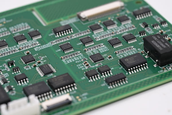
PCB prototype assembly is the small-volume process of fabricating a bare board, sourcing its components, mounting and soldering those parts, and inspecting and testing the completed assembly. The output is a physical PCBA that exposes design risks a schematic review cannot reveal, including footprint errors, thermal imbalance, inaccessible test nodes, assembly shadowing, and real signal or power behavior.
Bare-board fabrication and PCB prototype assembly are therefore different deliverables. Fabrication creates the conductive structure, solder mask, legend, holes, and finish. Assembly adds the electronic and electromechanical parts through surface-mount technology, through-hole technology, or a mixed process. A turnkey build can also include parts procurement, programming, and project-specific functional testing.
The goal is not to imitate high-volume output at any cost. A good PCB prototype assembly preserves the intended production materials and processes closely enough to expose risk, while keeping fixture investment and order quantity appropriate for a design that may still change.
Designing for PCB Prototype Assembly
A PCB designed for PCB prototype assembly must satisfy electrical intent and the physical process window of fabrication, solder paste printing, placement, reflow, inspection, and test. Completing this work before release shortens PCB prototype assembly more effectively than asking an assembler to recover an incomplete data package.
Component Placement for PCB Prototype Assembly
PCB prototype assembly benefits from components placed in functional blocks, decoupling capacitors kept close to their power pins, and clear access for rework and probing. Orient repeated parts consistently, mark polarized components clearly, and keep tall components away from areas that need optical inspection or selective soldering access.
For a fine-pitch BGA, begin with the escape-routing strategy rather than fitting the package after the rest of the board is routed. Confirm pad geometry, solder mask definition, via structure, finished surface, stencil approach, and X-ray coverage with the assembler. If via-in-pad is required, specify the filling and capping process; an open via can drain solder from a BGA joint and create intermittent opens.
Trace Width Spacing and Test Access for PCB Prototype Assembly
For PCB prototype assembly, set trace width from current, copper thickness, allowed temperature rise, and impedance requirements rather than from the factory minimum alone. Spacing must also consider voltage, contamination risk, solder mask registration, and the etching margin associated with copper weight. A capability limit is a boundary, not a preferred design rule.
Add accessible test points for power rails, grounds, reset, programming, communication buses, and critical analog nodes. PCB prototype assembly often uses flying probe testing because it avoids a dedicated fixture, but deliberate test access still improves coverage and diagnosis.
Layer Stackup for PCB Prototype Assembly
Define the PCB prototype assembly stackup before detailed routing when the board contains controlled impedance, fast edge rates, dense BGA fan-out, or sensitive analog circuits. Provide finished copper by layer, dielectric targets, impedance values and tolerances, and any back-drill or via-stub constraints. Pair signal layers with continuous reference planes and keep copper distribution reasonably balanced to reduce warpage.
PCB Prototype Assembly Design Rule Checks
The final DRC should include assembly checks as well as electrical clearance. The following release package prevents the most common version and interpretation errors in PCB prototype assembly.
| Release item | What to verify | Why it matters |
|---|---|---|
| Fabrication data | Gerbers or approved intelligent data, NC drill files, board outline, stackup, impedance table, and fabrication drawing agree on the same revision. | Prevents missing layers, wrong drills, and PCB prototype assembly stackup assumptions. |
| BOM | Manufacturer part number, description, package, quantity, approved alternates, do-not-fit status, and lifecycle risk are explicit. | Avoids sourcing substitutions and footprint mismatches. |
| Placement data | CPL coordinates, rotation, side, origin, and designators match the PCB prototype assembly drawing and BOM. | Prevents mirrored or rotated placement. |
| Assembly notes | Polarity, hand-solder items, thermal limits, press-fit parts, conformal coating keep-outs, and special cleaning are stated. | Turns design intent into repeatable work instructions. |
| Test package | Netlist, programming files, current limits, test sequence, expected readings, and pass or fail limits are version controlled. | Makes functional results comparable across revisions. |
PCBgogo PCB Prototype Assembly Process
PCBgogo PCB prototype assembly combines bare-board production, component sourcing, SMT or through-hole assembly, and staged inspection in one workflow. Keeping these stages under one order reduces handoff risk because fabrication data, BOM data, and placement data can be checked against the same revision.
PCB Fabrication for PCB Prototype Assembly
Engineers first review the fabrication package for manufacturability, then prepare the working panel and process data. Imaging, lamination, drilling, desmear, copper deposition and plating, solder mask, surface finish, legend, profiling, and electrical test follow the construction selected for the PCB prototype assembly. For controlled-impedance or HDI designs, stackup and microvia feasibility should be resolved before the board enters production.
Component Sourcing for PCB Prototype Assembly
PCB prototype assembly sourcing starts with a BOM that identifies exact manufacturer part numbers and approved alternatives. PCBgogo supports full turnkey, partial turnkey, and kitted or consigned models. Incoming quality control checks package and value against the order, while moisture-sensitive parts should be stored and handled according to their specified floor-life controls.
For PCB prototype assembly, availability often matters as much as unit price. If an alternate changes package height, thermal pad geometry, pin function, or electrical performance, it requires engineering approval rather than a purchasing-only substitution.
PCB Prototype Assembly Technologies and Steps
PCB prototype assembly uses SMT, through-hole, or mixed technology according to package type and product requirements. An automated SMT line typically prints paste through a laser-cut stencil, verifies paste deposition with SPI, places parts under machine vision, and solders them through a controlled reflow profile. Through-hole parts can then be inserted and soldered by selective, wave, or manual processes where appropriate.
Solder paste printing. Control aperture design, alignment, paste condition, and deposited volume before parts are placed.
SPI and first article. Measure paste deposits and confirm component values, orientation, and placement on the first build.
Automated placement. Load reels, trays, tubes, or cut tape; verify package recognition; and place components from the approved CPL file.
Reflow and through-hole. Run the qualified thermal profile, then complete THT, selective soldering, hand soldering, and cleaning as specified.
Programming and finishing. Program devices, apply coating or other post-assembly operations, and protect the finished PCBA for handling and shipment.
Inspection During PCB Prototype Assembly
Inspection is distributed through the PCB prototype assembly process rather than postponed until the end. SPI catches paste defects before placement; AOI checks component presence, polarity, alignment, and visible solder joints; X-ray examines hidden BGA and QFN connections. Electrical and functional tests then address defects that optical systems cannot prove.
PCB Prototype Assembly Testing Methods
PCB prototype assembly testing should separate workmanship defects from design behavior. No single method provides full coverage, so the test plan should combine structural inspection, electrical access, and functional exercise according to the failure risks of the product.
| Method | Best use | What it can reveal | Key limit |
|---|---|---|---|
| Visual inspection | First article and final workmanship | Wrong orientation, damage, poor wetting, contamination, label issues | Cannot assess hidden joints or prove circuit behavior |
| AOI | Repeatable SMT screening | Missing or shifted parts, polarity, bridges, visible solder defects | Depends on line of sight and programmed criteria |
| X-ray | BGA, QFN, LGA, and hidden joints | Bridging, void patterns, head-in-pillow indicators, missing balls | Does not prove firmware or complete function |
| Flying probe | Prototype and low-volume electrical test | Opens, shorts, continuity, and selected component measurements without a fixture | Slower per board and limited by accessible nodes |
| Bed of nails ICT | Stable designs and repeated volume | Fast component-level and net-level screening | Requires fixture cost and designed test access |
| Functional test | System-level acceptance | Power sequence, interfaces, sensors, outputs, firmware, and load response | Coverage is only as good as the written procedure and limits |
Begin first power-up with a current-limited supply, known-safe firmware, and a written sequence. Measure resistance to ground on each rail before applying power, then verify rail order, inrush current, clocks, reset, programming access, and thermal behavior before connecting external loads. This approach makes a PCB prototype assembly failure easier to isolate and safer to reproduce.
PCB Prototype Assembly Validation
PCB prototype assembly validation determines whether the finished PCBA meets defined requirements, not whether one board appears to work. Before the build, convert product needs into measurable acceptance criteria for voltage, current, timing, temperature, signal quality, mechanical fit, firmware behavior, and test coverage.
Electrical performance: Record rail margins, ripple, interface timing, analog accuracy, EMC-sensitive nodes, and operation at minimum and maximum input conditions.
Thermal performance: Measure component and board temperatures at representative load, ambient, airflow, and enclosure conditions rather than on an open bench only.
Mechanical integration: Confirm connector access, component height, mounting holes, keep-outs, enclosure clearance, cable strain, and depanelization edges.
Repeatability: Compare several assemblies and separate a design-wide pattern from one workmanship defect or damaged component.
Manufacturing evidence: Review AOI, X-ray, electrical, rework, and failure records to decide whether the PCB prototype assembly process is stable enough to repeat.
A validation report should identify the board revision, BOM revision, firmware version, test setup, equipment, limits, results, failures, and disposition. Without that traceability, later PCB prototype assembly results cannot be compared reliably.
PCB Prototype Assembly Iteration and Design Optimization
Iterative prototyping converts each PCB prototype assembly result into a controlled design change. The fastest teams do not change several unrelated variables and hope the next build works; they link every modification to evidence, an owner, and a verification test.
Classify the issue. Separate schematic, layout, component, fabrication, assembly, firmware, test, and user-interface causes.
Preserve evidence. Keep failed units, photographs, X-ray images, measurements, serial numbers, and rework history.
Define the smallest correction. Change only what is needed to test the root-cause hypothesis and update all affected outputs together.
Run DRC and DFM again. A local fix can create a new clearance, thermal, stencil, or test-access problem elsewhere.
Verify the revision. Repeat the failed test plus regression tests for functions that the correction could disturb.
Use an engineering change record that ties the schematic, layout, Gerbers, drill files, BOM, CPL, assembly drawing, firmware, and test procedure to one revision. A golden sample can guide visual comparison, but the controlled data package remains the manufacturing authority for the next PCB prototype assembly.
From PCB Prototype Assembly to Mass Production
A PCB prototype assembly is ready to move toward mass production when the design is repeatable, the supply chain is qualified, and the test process can distinguish a good unit from a bad one. Passing a demonstration is not enough; the release must survive normal material, process, and operator variation.
Freeze the product baseline: Approve the schematic, layout, stackup, BOM, alternates, firmware, drawings, and acceptance criteria as one release.
Run a pilot lot: Use production-intent panels, stencil, feeders, thermal profile, inspection programs, and packaging to expose scaling issues.
Qualify the BOM: Resolve lifecycle and lead-time risks, approve alternates through engineering, and define traceability for critical parts.
Convert learning into controls: Turn prototype rework notes into DFM rules, work instructions, AOI or X-ray criteria, and test limits.
Review yield by defect class: Track first-pass yield, rework, false failures, and escapes; do not hide recurring defects inside an overall pass percentage.
The handoff is complete only when the production team can build and test the board without relying on unwritten knowledge from the prototype engineer. Using the same manufacturing partner for PCB prototype assembly and ramp-up can reduce data translation, but revision control and pilot evidence are still essential.
Standards for PCB Prototype Assembly
PCB prototype standards define design practice, fabrication performance, workmanship, soldering, and acceptance; they do not replace project-specific requirements. Select the class and criteria from the product risk, operating environment, regulatory path, and customer contract.
| Standard | Role in PCB prototype assembly |
|---|---|
| IPC-2221 | General PCB design principles, including spacing, conductor, material, and mechanical considerations. |
| IPC-7351 | Land-pattern guidance for surface-mount components and assembly geometry. |
| IPC-6012 | Qualification and performance requirements for rigid printed boards, including Class 2 and Class 3 constructions. |
| IPC-A-600 | Visual acceptance criteria for bare printed boards. |
| IPC J-STD-001 | Requirements for soldered electrical and electronic assemblies, including process control and workmanship. |
| IPC-A-610 | Acceptance criteria for completed electronic assemblies; the applicable class must be agreed before production. |
| J-STD-020 and J-STD-033 | Moisture sensitivity classification, reflow exposure, storage, baking, and handling for sensitive packages. |
A purchase order should state the required standard, revision, class, special tests, documentation, and any precedence between the drawing and the standard. This prevents the PCB prototype assembly supplier from guessing which acceptance level applies.
Common PCB Prototype Assembly Challenges and Solutions
The most expensive PCB prototype assembly problems usually begin before the line starts. They arise from mismatched data, design features operating at the edge of a process, unqualified substitutions, or tests that cannot isolate the actual failure.
| Challenge | Likely cause | Practical solution |
|---|---|---|
| The quote or build is held | Gerber, BOM, CPL, drawing, or revision data conflict | Export all files from the released CAD revision, use one origin, and run a designator and quantity cross-check before upload. |
| Fine-pitch BGA opens or bridges | Pad, mask, via-in-pad, stencil, warpage, or reflow process is not matched to the package | Review the escape and land pattern with the assembler, specify filled and capped vias where needed, and require X-ray criteria. |
| Tombstoned passives | Unequal pad geometry or thermal mass causes one end to wet first | Balance pad connections, use thermal relief where appropriate, verify stencil apertures, and review the reflow profile. |
| Parts are unavailable | Single-source BOM, obsolete part, or unapproved substitute | Add qualified alternates early and require engineering approval for any change affecting fit, form, or function. |
| Board passes bench test but fails in product | Open-bench conditions do not represent enclosure, load, cable, or environment | Validate the PCB prototype assembly in the actual mechanical and thermal configuration with defined limits. |
| Failure cannot be isolated | No test points, no current limits, weak logging, or undocumented rework | Design for test, record serial-level results, and preserve failed units and inspection evidence. |
| Prototype works but pilot yield falls | Manual prototype process or rework masked a design that is not production-capable | Use production-intent stencil, panel, profile, inspection, and test during the pilot build. |
A Trusted PCB Prototype Assembly Partner
A PCB prototype assembly partner should support the first engineering sample and preserve the process knowledge needed for the next revision and production ramp. PCBgogo combines one-piece ordering, fabrication, component sourcing, automated SMT, inspection, and engineering review within one service.
Prototype quantity and speed: Orders can start at one piece. PCBgogo publishes a 24-hour expedited option for eligible work and lists three to four days as the normal prototype assembly lead time, subject to design and parts readiness.
Advanced PCB fabrication: Published prototype limits include up to 40 rigid layers, a 0.075 mm laser microvia, a 0.125 mm finished mechanical hole, 2.5/2.5 mil inner trace and space at 1/3 or 1/2 oz copper, and controlled impedance of plus or minus 5 ohms at 50 ohms or below and plus or minus 10 percent above 50 ohms.
Automated SMT precision: The assembly line supports 01005 components measuring 0.4 by 0.2 mm, BGA pitch down to 0.2 mm, and published placement capability of plus or minus 0.035 mm, with plus or minus 0.025 mm shown for 100FP at Cpk at least 1.0 under the stated three-sigma condition.
Inspection across the process: Incoming inspection and first-article LCR checks are followed by SPI, AOI, X-ray for hidden joints, flying probe or bed-of-nails electrical test, visual inspection, functional testing, and outgoing QA as the project requires.
Measured yield improvement: PCBgogo documents a DFM-optimized instrumentation project in which mass-production yield rose from 74 percent to 99 percent. That result is evidence from a defined case, not a blanket guarantee for every design.
Standards and quality systems: PCBgogo lists IPC-A-610 as its assembly quality grade and operates quality systems that include ISO 9001, IATF 16949, ISO 13485, ISO 14001, and ISO 45001 within their applicable scopes.
Engineering support: DFM and design review can address stackup, trace and spacing margins, drill aspect ratio, BGA fan-out, panelization, assembly access, testability, and the changes needed to move a PCB prototype assembly into repeat production.
These published values are process boundaries rather than universal design targets. Share the complete data package and intended volume so PCBgogo engineers can confirm which combination of materials, geometry, assembly, inspection, and lead time applies to the specific PCB prototype assembly.
PCBgogo - Reliable, High-Quality PCB Manufacturing
PCBgogo is a one-stop PCB and PCBA manufacturing factory, helping you save time and costs while ensuring consistent, reliable quality.
Get a Free Quote >
PCB Prototype Assembly Summary and Next Step
Successful PCB prototype assembly depends on a synchronized design package, production-representative assembly, layered inspection, measurable validation, and disciplined revision control. Those controls turn a working board into evidence that the product can be built again.
When the design is ready, submit the fabrication files, BOM, CPL data, assembly drawing, and test requirements to PCBgogo for engineering review and quotation. PCBgogo provides cost-effective PCB manufacturing and assembly from one-piece prototypes through volume production, with the process options and inspection coverage needed to protect product quality.
Frequently Asked Questions
What files are required for PCB prototype assembly?
At minimum, provide fabrication files and drills, a BOM with exact manufacturer part numbers, a CPL or pick-and-place file, and an assembly drawing. Add the stackup, impedance table, netlist, programming files, and functional test procedure when the design requires them.
How many boards should be built in the first prototype run?
Build enough PCB prototype assembly units to support destructive investigation, rework, firmware development, and repeatability checks. One board can demonstrate a function, but it cannot show whether a result is consistent across assemblies.
Can a fine pitch BGA be used in a PCB prototype assembly?
Yes, provided the pad design, stackup, via strategy, stencil, placement, reflow, and X-ray plan are compatible with the package. Confirm the complete geometry with the assembler before routing because package pitch alone does not determine manufacturability.
What is the best electrical test for a prototype?
Flying probe is often the practical starting point for PCB prototype assembly because it needs no dedicated fixture and can follow design revisions. It should be combined with AOI or X-ray and a functional test when the risk includes hidden joints or system behavior.
When is a PCB prototype ready for mass production?
A PCB prototype assembly is ready when the design meets measurable requirements across multiple assemblies, the BOM and alternates are qualified, and a pilot lot proves the production-intent process and test coverage. All released files must share the same controlled revision.
Does fast PCB prototype assembly reduce quality?
Not inherently. Speed is safe when files are complete, materials are available, and inspection gates are preserved; skipping DFM, SPI, X-ray, electrical test, or functional acceptance simply moves risk downstream.