
 日本語
日本語
 한국어
한국어

PCB Inner Layer Process: PCBgogo’s Precision Manufacturing
In a multilayer PCB, the inner layers do the work that no one sees after the board is finished. Before lamination, each core must already have the correct circuit pattern, copper thickness, and layer alignment because once the stackup is pressed together, those traces are permanently embedded inside the board.
This is why the inner layer process requires much tighter control than simply transferring an image onto copper. From imaging and etching to AOI inspection and oxide treatment, every step is designed to prevent defects that cannot be repaired later. In this guide, I’ll walk through the complete PCB inner layer manufacturing process and explain the four key factors that determine multilayer and HDI board reliability: compensation, copper thickness control, layer registration, and defect detection.
What Is a PCB Inner Layer Circuit?
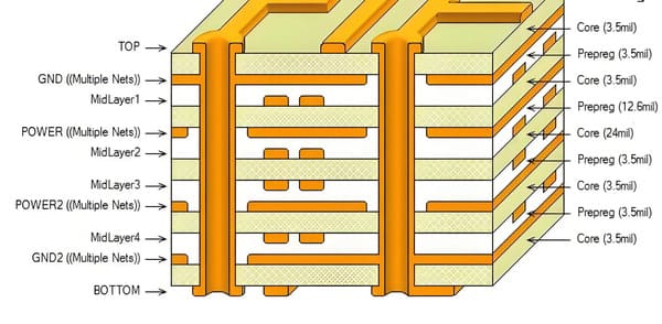
A PCB inner layer circuit is the copper pattern etched onto a copper-clad laminate core that will be buried inside a multilayer board. A four-layer board starts as one core carrying layers 2 and 3; a ten-layer board might start as four cores. Inner layers usually carry ground and power planes and buried routing.
The inner layer process is not the outer layer process done earlier. Four differences change the economics:
| Attribute | Inner Layer | Outer Layer |
|---|---|---|
| Copper Build | Etched from bonded foil. No plating, so foil weight is a hard ceiling. | Foil plus plated copper, so thickness is built up. |
| Image Polarity | Signal positive; plane layers may be negative artwork. | Almost always positive artwork. |
| Rework | None after lamination: scrap the core or lose the panel. | Most defects can be reworked. |
| Registration | Depends where each core lands after the material moves in the press. | Imaged onto the drilled panel against fiducials. |
This is why inner layer control is so important. Defects caught before lamination can usually be isolated to a single core, but once the stackup is pressed together, any hidden inner layer issue can affect the entire board.
The Multilayer PCB Inner Layer Process, Step by Step
The inner layer process may look straightforward on paper, but every step affects the accuracy and reliability of the final multilayer PCB. Starting from the copper-clad core, the process involves imaging, etching, inspection, and surface preparation before the layers can be pressed together. Let's walk through each step and see how a bare core becomes a finished inner layer ready for lamination.
| # | Step | Primary Failure Mode |
|---|---|---|
| 1 | Core cut and surface pre-treatment | Resist lifting, film wrinkles |
| 2 | Dry film lamination | Trapped particles, voids, poor tack |
| 3 | Exposure | Registration shift, under- or over-exposure |
| 4 | Developing | Residual resist, over-development |
| 5 | Etching | Over-etch, under-etch, undercut |
| 6 | Stripping | Resist residue on copper |
| 7 | Inner layer AOI | Escaped opens, shorts, nicks |
| 8 | Post-etch punch | Tooling error propagates to every layer |
| 9 | Brown oxide treatment | Weak bond, delamination, pink ring |
| 10 | Bake and lay-up | Oxidation, contamination, misordered stack |
PCB Inner Layer Exposure
After the copper is cleaned and dry film is hot-roll laminated onto it, exposure polymerises the resist in the pattern of the circuit. A film phototool is aligned mechanically and flooded with UV: fast and cheap, but the artwork expands and contracts with temperature and humidity, and it has one fixed size. Laser direct imaging (LDI) writes the pattern directly from CAM data with no physical mask.
The critical advantage of LDI on multilayer work is not resolution; it is adaptive scaling. An LDI system measures the actual panel, then writes the image scaled to that specific panel. On a twelve-layer board where every core has moved slightly differently, that is the difference between holding registration and losing the panel. Below roughly 3 mil line and space, and on any HDI build, LDI stops being an upgrade and becomes a requirement.

PCB Inner Layer Developing
Developing washes away unpolymerised resist with a mild alkaline spray. It is controlled by break point: the position along the chamber at which resist has just fully cleared, targeted near the midpoint. Too early and the image sits in fresh solution too long, rounding corners; too late and residual resist survives into etching, leaving copper slivers. Break point drifts as developer loads, so it is checked every shift.
PCB Inner Layer Etching
Etching dissolves all copper not protected by resist, almost always in an acidic cupric chloride line, which etches predictably and regenerates continuously. It is never purely vertical: as the etchant works downward, it also works sideways under the resist edge, producing a trapezoidal cross-section.
Etch factor = copper thickness ÷ undercut per side A well-controlled spray etch line on standard inner copper typically achieves 3:1 to 4:1. Heavier copper, slower conveyor speed and poorer agitation push it down, widening undercut and narrowing the finished trace. |
Etch factor is the number your fabricator uses to decide how much wider than nominal to draw your traces. Control variables are etchant concentration, temperature, conveyor speed, spray uniformity, and copper loading. That last one is a design issue: large pours next to fine-line areas etch unevenly, because the etchant is locally depleted where there is more copper to remove.
PCB Inner Layer AOI Inspection
Automated optical inspection is the last chance to catch a defect while the fix costs one core instead of a finished panel. The scanner compares the etched core against a reference derived from the same CAM data used to expose it, and applies geometric checks for minimum width, spacing and annular ring.
It detects opens including partial opens, shorts and copper bridges, nicks and mouse bites, copper residue, protrusions and slivers, pinholes in planes, and line width or spacing outside tolerance.
AOI produces coordinates, not verdicts. Flagged sites go to a verify station where an operator classifies each as a genuine defect, a false call, or cosmetic. Excess copper can sometimes be removed mechanically and re-inspected, but an inner layer open is usually a scrap decision, because no repair can be verified after lamination. A nick acceptable on a plane is unacceptable on a controlled impedance trace, which is why layer function belongs in your fabrication notes.
Post-Etch Punch and Registration Tooling
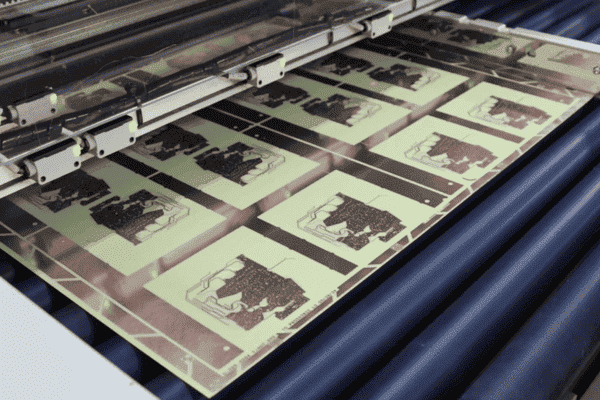
Each core is then punched with lamination tooling holes. Punching at a fixed position would permanently lock in whatever misalignment that core already carries. Post-etch punch systems instead optically locate registration targets etched into the copper as part of the circuit image and punch relative to it, so every core is referenced to its own circuitry and misregistration is reduced to residual rather than accumulated error.
PCB Inner Layer Brown Oxide Treatment
Bare, smooth copper does not bond reliably to epoxy prepreg. Brown oxide treatment, or browning, converts the surface into a micro-roughened, chemically compatible layer that resin keys into, and it decides whether your board delaminates. A horizontal line runs through cleaning, acid micro-etch, pre-dip, adhesion promotion, and controlled drying.
Browning replaced black oxide because black oxide builds a thicker, brittle layer vulnerable to acid attack at drilled holes, producing a pink ring. Note the high-frequency trade-off: more roughness bonds better but raises conductor loss through the skin effect, which is why high-speed designs move toward low-profile foil.
PCB Inner Layer Pre-Lamination Preparation
Browned cores are perishable: the treated surface oxidises and absorbs moisture, so fabs enforce a time window between browning and pressing, and cores that exceed it are re-browned. Cores are baked first, since trapped water flashes to steam at press temperature and creates voids.
Lay-up then builds the book on tooling pins. Three things decide the outcome: prepreg resin content must fill the etched-away areas of each layer; the stack must be symmetric or the panel bows as it cools; and layer order and orientation must be verified, since a core loaded upside down produces a mirrored layer.
PCB Inner Layer Line Width Compensation
Your Gerber file says 5 mil; the production data says something wider. That is not an error. Two independent compensations are applied to every inner layer.
Etch compensation. Because etching undercuts the resist, CAM enlarges the conductor by the expected undercut per side. As a first-order estimate, undercut per side equals copper thickness divided by etch factor: on 1 oz (35 μm) inner copper at etch factor 3, roughly 12 μm per side, about 1 mil on total width. Heavier copper takes longer to etch through, so compensation grows — which is why the same fabricator quotes finer minimum lines on 0.5 oz inner copper than on 2 oz.
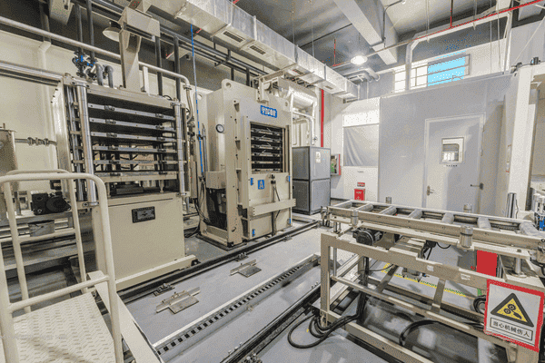
Scaling compensation. Laminate moves dimensionally during lamination as etched-in stress releases and resin cures. Fabricators pre-scale the inner layer artwork so that after the panel moves, features land where the drill program expects. Scaling factors are established empirically per material, copper distribution and stack-up, and differ between X and Y because woven glass is not isotropic.
Two rules follow. Do not pre-compensate your artwork, or the fab's compensation lands on top of yours. And keep copper balanced: scaling is one average correction that cannot fix a local anomaly.
PCB Inner Layer Copper Thickness Control
Outer copper is built up: the foil is plated during through-hole metallisation, so it finishes thicker than it started. Inner layers receive no plating at all — finished inner copper is the original clad foil minus whatever pre-treatment, etching and browning consumed.
Foil weight is a hard ceiling. Specify 1 oz inner copper, and you will never measure more than 1 oz.
Finished copper sits slightly below nominal, since each chemical step removes a little, so impedance models assuming full nominal thickness run marginally optimistic.
Inner copper is more uniform than outer copper, having never seen plating distribution effects — one reason controlled impedance is easier to hold on buried striplines than surface microstrips.
Copper weight and impedance are coupled. Stripline impedance depends on conductor thickness as well as width and dielectric height, so changing inner copper from 1 oz to 1.5 oz without re-solving the stack-up moves impedance off target. For current capacity, use planes rather than heavy copper traces.
PCB Layer Registration Accuracy
Layer registration accuracy measures how well every layer lines up with the others and with the drilled holes. It limits achievable layer count and annular ring, and error comes from independent sources that each consume part of a budget:
| Error Source | Contribution | Controlled By |
|---|---|---|
| Artwork or LDI accuracy | Small on LDI, larger on drifted film | Environmental control; per-panel fiducials |
| Post-etch punch | Small when referencing etched targets | Optical targets, not fixed-position tooling |
| Material movement in lamination | Usually the largest contributor | Scaling per stack-up; balanced copper |
| Drill position accuracy | Small on maintained equipment | X-ray target location; calibration |
Fabricators control this with etched targets, post-etch punch referenced to them, per-stack-up scaling, and X-ray target drilling that locates buried targets through the pressed panel so residual error spreads evenly. On HDI builds, registration is re-established at every lamination cycle.
Designers control the rest: generous inner layer antipads, balanced copper so scaling works, a symmetric stack-up, and critical features declared in the fabrication notes. Fabricators typically require larger hole-to-copper clearance on inner layers than outer ones, precisely because inner layers carry the registration penalty.
HDI PCB Inner Layer Process
HDI does not replace the inner layer process; it runs it more times, on thinner material, with less margin. A conventional board is pressed once. An HDI board is built up sequentially: a core is processed, pressed with additional layers, laser-drilled, plated, imaged, then pressed again. 1+N+1 adds one build-up layer per side, 2+N+2 adds two.
Each cycle is another chance for material to move and another registration budget to spend, and copper inside the board sees multiple thermal cycles, so resin selection matters more than on a single-press board. HDI cores can be a fraction of conventional thickness, at which point laminate stops behaving like a rigid panel.
| Process Element | Conventional Multilayer | HDI |
|---|---|---|
| Imaging | Film phototool workable | LDI effectively mandatory |
| Copper Foil | Standard profile acceptable | Thin, low-profile foil for etchability and loss |
| Lamination Cycles | One | Multiple, registration re-established each time |
| Via Formation | Mechanical drilling | Laser microvias, often stacked or staggered |
| Inner Layer AOI | Standard resolution | Higher resolution, tighter thresholds |
Defect severity in HDI scales with feature size, not defect size. A 1 mil nick removes 17% of a 6 mil trace and is often acceptable; the same defect halves a 2 mil trace and is a reject. An escape that loses a six-layer panel after one press loses an HDI panel after several presses, platings and laser drills.
PCB Inner Layer Defects: Opens, Shorts and Prevention
Opens and shorts make a board non-functional rather than merely out of specification. Inner layer opens usually trace back to a particle or void in the dry film, over-etching that severed a marginal trace, a scratch in the resist, or a plane split connected only through a copper bridge too narrow to survive etch compensation. Shorts come from the opposite direction: incomplete development, contamination masking copper, under-etching from a depleted or cold etchant, or spacing too tight for the etchant to reach into.
The asymmetry matters. A short is often repairable by removing excess copper under a microscope; an inner layer open generally is not, which is why fabs tune inner layer etching slightly conservatively. It is also why electrical test cannot save you: E-test confirms an open exists, but only core-stage optical inspection prevents one.
| Defect | Typical Cause | Prevention |
|---|---|---|
| Open Circuit | Dry film void or scratch; over-etch; narrow plane-split bridge | Cleanroom discipline; etch rate control; no narrow bridges |
| Short Circuit | Under-etch; incomplete development; contamination | Break point control; etchant maintenance; adequate spacing |
| Nick / Mouse Bite | Localised over-etch; small resist defect | Spray uniformity; film handling; AOI thresholds per feature |
| Copper Residue | Under-etch in a locally depleted area | Balanced copper; no large pours beside fine lines |
| Delamination | Inadequate browning; moisture; exceeded window | Browning control; bake before lay-up |
| Pink Ring | Bond failure at a hole allowing acid attack | Acid-resistant browning; desmear and plating control |
Design Rules That Protect Inner Layer Yield
Design above the fab's minimum, not at it, and widen inner layer clearances around drilled holes. Antipads absorb registration error — the cheapest insurance on a multilayer board.
Never connect a net through a single narrow copper bridge. A bridge in a dense BGA fan-out that is barely wide enough on paper may not survive etch compensation.
Balance copper across and between layers, and keep the stack-up symmetric in both dielectric thickness and copper weight. Add thieving in large empty areas.
Do not mix very fine lines with large copper pours on one layer. Local etchant depletion leaves residue and uneven line width.
Specify copper weight and impedance together, and submit true nominal geometry.
Check inner layer polarity before you order. Open every layer in a Gerber viewer and confirm plane layers render as intended. An inverted plane layer is the most expensive file error in multilayer fabrication, and it stays invisible until the boards fail test.
Inner Layer Capability at PCBgogo
Published inner layer parameters are the fastest way to tell whether a fabricator can build your stack-up. Below are PCBgogo's stated capabilities.
| Parameter | Standard FR-4 | Advanced / HDI |
|---|---|---|
| Layer Count | 1, 2, 4, 6, 8, 10 layers | 1–40 layers |
| Inner Layer Copper Thickness | 1 oz / 1.5 oz (35 μm / 50 μm) | Finished copper 0.5–6 oz |
| Inner Layer Min Track / Spacing | ≥ 4 mil | 2 / 2 mil |
| Outer Layer Min Track / Spacing | ≥ 3 mil | 2.5 / 2.5 mil |
| Min Spacing, Hole to Inner Conductor | — | 7 mil (outer layer: 6 mil) |
| Circuit Imaging Method | — | Film or LDI |
| HDI Construction | — | HDI 1–3 steps |
| Min BGA Pitch | — | 0.1 mm |
At PCBgogo, we understand that inner layer defects are some of the most costly PCB failures. That's why we focus on catching issues before the layers are bonded together, with DFM review, controlled imaging and etching, AOI inspection, and inner layer testing to detect potential opens, shorts, and alignment problems early.
Before production, you can also use the PCBgogo Gerber Viewer to check your layer stackup, inner layer polarity, and design data online without installing software. With multilayer and HDI PCB manufacturing capabilities, ISO 9001:2015 and UL-certified production, PCBgogo helps reduce inner layer risks and deliver reliable boards for your applications.
Frequently Asked Questions
Can inner layer defects be repaired after lamination?
No. Once cores are pressed, inner layer circuitry is sealed in cured resin with no physical or optical access, so a defect found afterwards means the panel is scrapped.
Why is my inner layer trace narrower than I designed it?
Etching removes copper sideways as well as downward, so a trace finishes narrower than the opening in the photoresist. Fabricators compensate by enlarging conductors in the production data, but the result still shows a trapezoidal cross-section. If measured width is consistently below target, etch compensation for that copper weight is what to raise with your fabricator.
What is brown oxide treatment and why do inner layers need it?
Browning converts smooth inner layer copper into a micro-roughened, resin-compatible surface. Without it, prepreg does not bond reliably and the board can delaminate during reflow. It replaced black oxide because it resists acid attack at drilled holes better, reducing pink ring.
What is the difference between inner layer AOI and electrical test?
Inner layer AOI inspects the etched core against the CAM reference before lamination, catching defects while a rejected core costs one core. Electrical test runs on the finished board, after everything is permanent. AOI prevents inner layer scrap; E-test only detects it.





