




 日本語
日本語
 한국어
한국어

Hard Gold vs ENIG: Which PCB Finish Should You Choose?
KEY DEFINITION PCB gold plating is a surface finish that deposits gold, usually over a nickel barrier, onto contact areas like edge connectors, keypads, or bond pads. Hard (electrolytic) gold resists wear and suits repeated plugging; ENIG (immersion gold) is thinner and built for soldering. The right choice depends on whether the pad gets touched or soldered.
A board with an edge connector that gets plugged and unplugged a few hundred times starts showing intermittent connection failures after a few months in the field. Nine times out of ten, that's a finish problem, not a design problem: someone specified ENIG where the pad needed hard gold.
This covers the actual types of PCB gold plating, where each one belongs on a board, and what the thickness numbers on a fab drawing really mean.
Where PCB Gold Plating Actually Shows Up
Not every gold-colored pad on a board does the same job, and the application usually tells you which type of gold plating it needs.
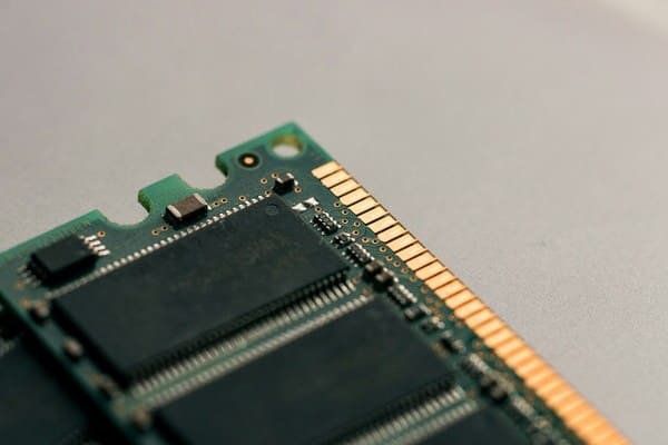
Memory and expansion cards: RAM modules, graphics cards, and PCIe add-in cards use gold fingers along the board edge because the connector gets reseated repeatedly over the product's life, and a soft finish would wear through in months.
Wearables and handheld electronics: smartwatches, fitness trackers, and handheld scanners rely on small board-to-board or battery connectors where a durable, low-resistance contact matters more than solder ease.
Industrial and test equipment interfaces: daughterboards and interface cards in factory-floor controllers and bench test gear get swapped or serviced often enough that a worn contact becomes a real failure mode, not a theoretical one.
Keypads and membrane switches: contacts that repeatedly meet conductive rubber need the same wear resistance as an edge connector, which is why they get the same hard gold finish.
RF and precision instrumentation: high-frequency boards use gold plating for its low, stable contact resistance, though at multi-gigahertz frequencies the plating's effect on signal integrity becomes its own design consideration, covered further down.
Once you know which category a pad falls into, the next question is which specific type of gold plating actually fits it, and that comes down to three real options.
The Three Types of PCB Gold Plating
Hard (Electrolytic) Gold
Hard gold is gold electroplated over a nickel barrier layer, usually alloyed with a small amount of cobalt or nickel to raise its hardness, and it's the finish behind every gold finger and gold-plated keypad contact.
The plating is specified under ASTM B488, which classifies electrodeposited gold coatings by purity (at least 99 percent gold) and by hardness, and commercial gold fingers typically run in the 30 to 50 microinch range over 100 to 200 microinches of nickel.
Soft (Flash) Gold
Soft gold is a much thinner, purer electroplated layer, generally left unalloyed, and it's the finish used for wire bonding rather than mechanical contact.
Because wire bonding needs a soft, ultra-pure surface for the bond wire to key into, this finish typically stays under a few microinches and is deliberately not built for wear resistance.
ENIG (Electroless Nickel Immersion Gold)
ENIG deposits nickel chemically rather than electrically, then displaces a thin immersion gold layer on top, and it's the finish most boards actually ship with because it solders well and stays flat at fine pitch.
The governing specification, IPC-4552, calls for a nickel layer of roughly 3 to 6 micrometers and a gold layer of only about 0.05 to 0.1 micrometers, thin enough that ENIG was never meant to survive repeated mechanical contact.
Lined up side by side, the differences between the three finishes come down to thickness, hardness, and whether the pad underneath is meant to be soldered or touched:
| Finish | Deposition | Typical Thickness | Hardness | Solderable | Best For |
|---|---|---|---|---|---|
| Hard gold | Electrolytic, alloyed | 30-50 uin over 100-200 uin Ni | High, wear-resistant | Poor | Edge connectors, keypads |
| Soft gold | Electrolytic, pure | A few uin | Low, soft | N/A (bonded) | Wire bonding, COB |
| ENIG | Electroless + immersion | ~2-4 uin Au over 3-6 um Ni | Low | Excellent | SMT pads, BGA, fine pitch |
Knowing the three types is only half the job. The harder part is matching the right one, and the right thickness, to what the board actually needs to survive.
What Actually Determines Which Gold Finish You Need
Skip the marketing language about which finish is "better" and look at what the pad is doing physically. That's what drives the choice, not preference.
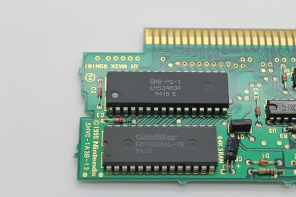
Whether the pad gets touched or soldered: solderable pads (SMT, BGA, through-hole) call for ENIG; mechanical contact points like edge connectors and switch contacts call for hard gold, since hard gold's poor solderability rules it out anywhere solder paste needs to wet the surface.
How many insertion cycles the connector needs to survive: a 30 microinch hard gold finger is commonly rated for roughly 1,000 insertion cycles in commercial designs, so a card that gets swapped daily in test equipment needs more margin than one seated once at assembly and left alone.
Whether the board mixes both jobs: a board with an edge connector and solderable pads on the same panel can't use a single blanket finish, since it needs hard gold on the fingers and something solderable everywhere else, which pushes the design toward selective or dual-section plating.
Signal frequency: at multi-gigahertz frequencies, current concentrates near the conductor surface (the skin effect), so the plating's uniformity and thickness start to affect impedance and loss, not just contact resistance, on high-speed edge connectors.
Cost and plated area: gold is the expensive part of any of these finishes, so most cost-conscious designs plate only the fingers or contact pads with hard gold and leave the rest of the board on a cheaper finish rather than gold-plating the entire surface.
These decisions only mean something if the finish that comes off the line actually matches the spec, which is where the industry's plating standards come in.
The Standards That Actually Govern Gold Plating Thickness
PCB gold plating isn't governed by a single certification. It's a stack of standards that each cover a different layer of the same finish.
ASTM B488: sets purity (minimum 99 percent gold) and hardness classifications for electrodeposited hard gold coatings, the standard fabricators cite for gold fingers and keypad contacts.
IPC-4552 (Revision B): specifies ENIG nickel and gold thickness ranges and, since its most recent revision, sets criteria for evaluating nickel corrosion, the root cause of black pad defects.
IPC-6012: the general PCB performance and qualification standard, ties gold finish thickness requirements to IPC Class 1, 2, or 3 designations based on the end product's reliability requirements.
None of these standards certify a finished board on their own. They define the acceptance criteria a fabricator's plating line and inspection process are supposed to hit, order after order.
What Actually Goes Wrong With Gold Plating
Most gold plating problems trace back to one of a few recurring failure modes, and a couple of longer-term shifts are changing how the industry handles them.
Black pad and nickel corrosion: excess gold thickness on ENIG can point to nickel that corroded during the immersion process, a defect that shows up as brittle solder joints months after assembly rather than at incoming inspection, which is why IPC-4552's later revisions added specific corrosion evaluation criteria.
Signal integrity at high frequency: as designs push into the multi-gigahertz range, gold plating's effect on impedance and skin-effect losses becomes a real constraint on ultra-fine line widths, not just a contact-resistance question.
Rising gold cost: with gold pricing what it is, selective plating (gold on only the fingers or contact pads rather than the whole board) has gone from a cost-saving option to close to the default approach on most commercial designs.
Fine-pitch adaptation: sub-0.4mm pitch components need an extremely flat pad surface, and immersion gold's chemical deposition process handles that flatness more consistently than older tin-based finishes could.
Cyanide-free plating chemistry: traditional gold plating baths use cyanide-based electrolytes, and environmental and worker-safety pressure has been pushing platers toward cyanide-free gold chemistries, though the older baths still dominate high-volume production.
Catching these issues before a board ships comes down to how tightly a fabricator controls the plating process and checks it, order by order.
How PCBgogo Handles Gold Finger and ENIG Orders on the Same Board
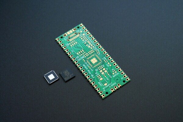
Boards that mix a hard-gold edge connector with solderable ENIG pads, the exact situation flagged above, are where finish selection actually gets tested in production, and it's worth knowing how a fabricator handles that combination before committing to a design. PCBgogo offers both electrolytic hard gold and ENIG as surface finish options on the same FR-4 order, so a board's edge connector and its solderable pads don't have to compromise on one finish.
Gold finger designs go through PCBgogo's per-order DFM and engineer review before fabrication, which is where issues like insufficient clearance around the fingers get caught before they turn into a respin.
PCBgogo's published gold finger design rules call for a minimum 1.0mm clearance between the fingers and the board outline, no plated through-holes within 1.0mm of the fingers, a minimum 1.0mm board thickness for gold finger boards, and 30-degree edge beveling.
Finished boards go through AOI and X-ray inspection, which is how dimensional and coverage issues on the plated fingers get caught before a batch ships rather than after a customer reports failures.
Production runs under IATF 16949 and ISO 9001 certification, which matters for repeat orders where the finish needs to come out identical from one batch to the next.
For a board that mixes both finishes, uploading the Gerbers to PCBgogo's online quoting tool gets a finish-specific DFM check before the order is placed.
Frequently Asked Questions
What is the difference between gold plating and gold flashing on a PCB?
"Gold plating" usually means electroplated hard gold, thick enough (commonly 30 to 50 microinches) to survive repeated contact. "Gold flashing," or soft gold, is a much thinner, purer layer used for wire bonding, not mechanical wear.
Can gold-plated pads be soldered?
Hard gold solders poorly because of its alloying elements and thickness, so it's used on connector fingers and keypads rather than solderable pads. ENIG, by contrast, is specifically designed to solder well.
How thick should PCB gold plating be?
It depends on the finish: hard gold fingers commonly run 30 to 50 microinches over 100 to 200 microinches of nickel, while ENIG's gold layer is typically only about 2 to 4 microinches under IPC-4552.
What is black pad, and does it affect hard gold plating?
Black pad is a nickel corrosion defect specific to ENIG, caused by an unstable immersion gold reaction. It isn't a risk with electrolytic hard gold, since that process doesn't rely on immersion chemistry.
Why do gold fingers need to be beveled?
Beveling the edge of a gold finger lets the connector slide into its socket without scraping or peeling the plated surface on insertion.
Is ENIG the same as gold plating?
ENIG technically is a form of gold plating, but in PCB shorthand "gold plating" almost always refers to the thicker electrolytic hard gold used on connectors, while ENIG is treated as its own separate finish category.
Match the Finish to the Pad, Not the Habit
Gold plating on a PCB isn't one finish; it's three different processes solving three different problems, and picking the wrong one shows up as a field failure months after the board ships, not on incoming inspection. Start from what each pad actually does, mechanical contact or solder joint, and the choice between hard gold, soft gold, and ENIG mostly makes itself. From there, a quick DFM check before fabrication is what catches any mismatch before it becomes a respin.





