
 日本語
日本語
 한국어
한국어

Why PCB Copper Plating Makes or Breaks Board Reliability?
QUICK ANSWER PCB copper plating is a two-stage process that starts with electroless copper deposition to create a conductive seed layer inside drilled holes, followed by electrolytic copper plating to build the copper thickness required for reliable connections. The process depends heavily on electrolyte chemistry, current density control, and hole-wall preparation, while final reliability also requires consistent copper distribution, adhesion, and grain structure verified through cross-section inspection.
What Copper Plating Actually Does in a PCB
A raw PCB substrate — FR-4, polyimide, or otherwise — is an insulator. Once holes are drilled for vias and through-holes, those hole walls are bare dielectric with no way to carry current between layers. Copper plating is the process that turns that insulating hole wall into a conductive path, and it's also the process that builds up the copper on traces and pads to the thickness a design actually needs.
It's easy to treat copper plating as a single step in a fabrication traveler. In practice, it's closer to a chemistry-and-electronics discipline of its own, with enough variables that two boards built to the same nominal spec can come out of the plating line with meaningfully different reliability — even when both pass a basic continuity test.
Stage One: Electroless Copper
Electroless (or 'chemical') copper plating deposits a very thin, uniform copper layer — typically under 1 μm — onto every exposed surface, including the insulating hole walls, without any applied current. It relies on an autocatalytic chemical reaction, usually preceded by a palladium activation step that gives the copper somewhere to start depositing.
This step gets far less attention than electrolytic plating because it's thin and largely invisible in a finished board's spec sheet. But it sets the ceiling for everything that follows: if the hole wall isn't fully cleaned of drilling smear and debris, or if the electroless layer is thin, patchy, or contaminated, no amount of electrolytic plating on top will fully compensate. Poor adhesion at this stage is one of the most common — and most preventable — root causes of later delamination and via barrel cracking.
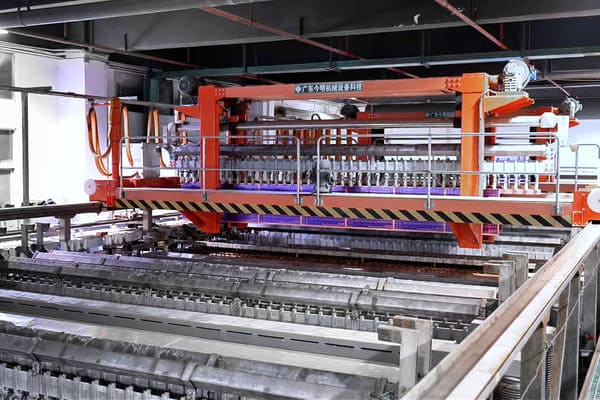
What Determines a Good Electroless Deposit
Desmear and etchback quality after drilling, removing resin smear left on the hole wall
Conditioning and micro-etch steps that give the copper something to mechanically key into
Catalyst (palladium) bath concentration and immersion time
Electroless bath stability — contamination or formaldehyde-based reducing agent drift both degrade uniformity
Stage Two: Electrolytic Copper Plating
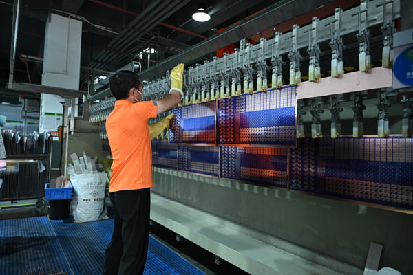
Electrolytic plating is what builds the seed layer up to functional thickness using an applied current in an acidic copper sulfate bath. This is where most of the copper mass in a via or trace actually comes from, and it's also where the majority of measurable process variation shows up on a finished panel.
Three variables do most of the work: copper sulfate concentration (which supplies the ions being deposited), current density (which controls deposition rate and, indirectly, grain structure), and organic additive balance — brighteners, levelers, and suppressors that control how evenly copper distributes across a panel, especially into high-aspect-ratio holes.
Why this matters for reliability: Copper deposited under an unstable or poorly balanced bath tends to form larger, less uniform grain structures. That copper is more brittle under thermal cycling — which is exactly the stress a plated through-hole experiences every time a board goes through reflow or operates through a wide temperature range in the field.
Why 20–25 μm, Specifically
20–25 μm didn't come from a whiteboard. It's the number IPC-6012 settled on for Class 2/3 through-hole and via plating after enough field failures pointed the same direction, and it's why via-in-pad now carries its own wrap-plating requirement: copper that stops abruptly at the hole edge instead of wrapping onto the annular ring kept showing up in the post-mortems on cracked barrels.
A connector manufacturer's own incoming-inspection data made the same point independently. Boards with wrap plating under spec accounted for a disproportionate share of their thermal-cycling failures — enough that they tightened the incoming spec past the IPC minimum rather than argue about it lot by lot.
Common Copper Plating Defects and Their Root Causes
Most copper plating defects trace back to a small number of process breakdowns. Recognizing the pattern speeds up root-cause diagnosis considerably:
| Defect | Typical Visual Signature | Most Common Root Cause |
|---|---|---|
| Nodulation / Roughness | Grainy, matte, sandpaper-like surface | Brightener or leveler depletion in the electrolytic bath |
| Voiding in Blind / Buried Vias | Gaps or thin spots visible on cross-section | Poor solution exchange in high aspect-ratio holes; trapped air |
| Barrel Cracking | Circumferential crack in the plated hole wall | Excessive thermal stress relative to copper ductility/thickness |
| Pink Ring / Etchback Residue | Pink discoloration around the hole after etch | Incomplete desmear leaving resin smear on the barrel wall |
| Edge / Corner Burn (Dark, Brittle Deposit) | Dark, rough patches at panel edges or high-current areas | Localized current density far above the process window |
| Post-plating Oxidation | Dulling or discoloration during storage | Surface finish applied too late, or inadequate finish for shelf life |
Case Study: Diagnosing Blind Via Voiding on a 10-Layer Industrial Controller Board
An industrial controls customer building a 10-layer motor controller board began seeing intermittent continuity failures during in-circuit test — not on every panel, but consistently clustered on boards from certain production lots. Cross-sectioning the failed units under microscope showed the problem: partial voiding inside blind vias connecting the outer layers to layer 3, with copper coverage dropping below the specified minimum in the deepest portion of several via barrels.
The failure pattern narrowed the search quickly. Voiding concentrated in blind vias rather than surface features pointed toward solution exchange rather than bath chemistry alone — high-aspect-ratio holes are the hardest features on a panel to keep supplied with fresh electrolyte, since fluid movement inside a narrow, non-through hole is limited by design.
What the Investigation Found
Panel agitation intervals during electrolytic plating were longer than optimal for the aspect ratio involved, allowing localized ion depletion inside the blind vias
Air entrapment during the initial bath immersion was not being fully addressed before current was applied
Current density was set for average panel conditions rather than adjusted for the higher-aspect-ratio blind via zones
Corrective Actions
Tightened agitation cycle frequency and added supplementary eductor agitation targeted at the blind via regions
Introduced a controlled pre-wetting/vacuum step before current initiation to reduce trapped air
Adjusted current density downward with extended plating time to prioritize uniform fill over plating speed
Added 100% X-ray sampling on blind via zones for the next three production lots to confirm the fix held
Follow-up cross-sections across the next lots showed voiding eliminated and copper coverage consistently above the specified minimum through the full via depth. The case is a useful reminder that copper plating problems are rarely solved by adjusting a single parameter — voiding, cracking, and adhesion failures each tend to have a distinct signature that points toward a specific stage of the process, and treating the wrong stage wastes a production cycle without fixing anything.
Quality Control: How Copper Plating Should Actually Be Verified
A visual pass and a basic continuity check are not sufficient evidence that copper plating meets spec — both can look fine on a board with marginal thickness or hidden voiding. Verification that actually catches these issues includes:
Microsection (cross-section) analysis — the only method that directly confirms thickness and coverage inside a via barrel, not just on the surface
Automated Optical Inspection (AOI) for surface-level defects across the full panel
X-ray inspection for internal via and buried structure integrity without destructive sectioning
Thermal stress testing (solder float or reflow simulation) to catch marginal adhesion before it becomes a field failure
Working With PCBgogo on Copper Plating-Critical Boards
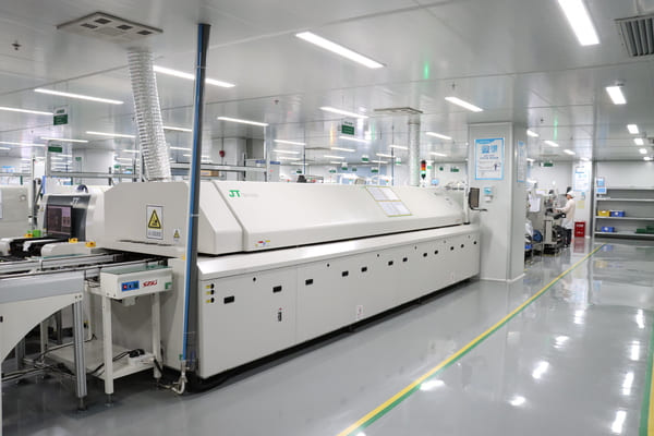
PCBgogo controls every critical stage of PCB production within its own manufacturing system, from drilling and copper plating to final surface finishing. By keeping these processes closely connected, PCBgogo delivers better consistency, tighter quality control, and more reliable boards for demanding applications.
Boards are built on Shengyi and Kingboard laminates, giving predictable thermal and dimensional behavior for plating and lamination
Layer counts up to 40 layers, with blind, buried, and via-in-pad structures supported for designs where wrap plating integrity matters
Surface finish options include ENIG, OSP, immersion silver, and chemical tin, selected based on the storage and assembly conditions a board will actually see
Every order goes through DFM and engineer review, plus AOI and X-ray inspection, before and after production
Manufacturing is certified to IATF 16949 and ISO 9001, with RoHS and UL compliance, backed by over a decade of production experience
A 24-hour expedited option is available for time-critical prototype or pilot runs
Native support for Eagle, Altium, and PADS files keeps DFM review tied directly to your original design intent
Get your PCB project moving today with PCBgogo's instant online quote tool. Simply upload your design files and requirements to receive a project-specific quote. If your board involves advanced technologies, tight tolerances, or unique requirements, contact our PCB experts for a tailored consultation.
Frequently Asked Questions
1. What is the difference between electroless and electrolytic copper plating?
Electroless copper is a thin, chemically deposited seed layer (roughly 0.5–1 μm) that makes an insulating hole wall conductive. Electrolytic copper plating then uses current to build that seed layer up to the final functional thickness on traces, pads, and via barrels.
2. How thick should copper plating be in a via or through-hole?
Most standard boards target 20–25 μm of plated copper in the hole wall, which aligns with common IPC-6012 Class 2/3 expectations; high-reliability or high-current designs may specify more.
3. Why do some PCBs develop copper cracking after thermal cycling?
Cracking usually points to a mismatch between plated copper ductility/thickness and the thermal stress the board sees in reflow or field use — often from bath chemistry drift, insufficient thickness, or an under-controlled current density during plating.
4. Can copper plating thickness vary across a single panel?
Yes. Current density is rarely perfectly uniform across a panel, especially near edges or dense feature areas, which is why manufacturers use thieving patterns, panel design rules, and thickness sampling rather than a single spot check.
5. Does surface finish affect copper plating reliability?
Indirectly, yes. The surface finish (ENIG, OSP, immersion silver, etc.) protects the plated copper from oxidation and mechanical damage after fabrication, so choosing the wrong finish for the storage or assembly environment can undermine otherwise well-plated copper.
6. How can I verify a supplier's copper plating quality before placing a production order?
Ask for microsection (cross-section) reports, AOI and X-ray inspection data, and their per-order DFM review process — reputable manufacturers will share this without hesitation, and most offer engineering review on request before you commit to a full run.





