
 日本語
日本語
 한국어
한국어

PCB Assembly Issues: Common Causes, Diagnosis, and How to Repair Them
Every PCB assembly run carries some risk of defects — even with a well-designed board, tight process control, and experienced operators. The difference between a minor hiccup and a costly failure usually comes down to how quickly an issue is identified, correctly diagnosed, and either repaired or escalated. This guide breaks down the most common PCB assembly issues, how they're diagnosed on the production floor and on the bench, practical repair techniques, and — just as importantly — when repairing a board isn't actually the right call.
Why PCB Assembly Issues Happen
Most assembly problems don't trace back to a single mistake — they're the result of a small gap somewhere upstream that only becomes visible once the board is populated and tested. Four areas tend to account for the majority of issues:
Design gaps: footprints, pad sizes, or component spacing that weren't reviewed for manufacturability before the board went to production.
Material issues: moisture-sensitive components that weren't stored or baked correctly, or solder paste that wasn't handled within its shelf life.
Process variation: reflow profiles that don't match the thermal requirements of every component on the board, or placement equipment that has drifted out of calibration.
Documentation gaps: an outdated BOM, a footprint that doesn't match the actual part, or a design revision that wasn't communicated to the assembly line.
Keeping these four categories in mind makes it much easier to trace a defect back to its actual cause instead of just treating the symptom.
The Most Common PCB Assembly Issues
The table below groups the defects you're most likely to run into by category, along with what each one typically looks like and its usual root cause.
| Issue | Category | What It Looks Like | Typical Root Cause |
|---|---|---|---|
| Cold solder joint | Soldering | Dull, grainy, or cracked joint; intermittent connection | Insufficient heat or time during reflow |
| Solder bridging | Soldering | Unintended connection between adjacent pads or pins | Excess paste volume or a misaligned stencil |
| Tombstoning | Soldering | Chip component stands up on one end after reflow | Uneven heating across the pads during reflow |
| Voids / insufficient solder | Soldering | Weak or hollow joint, often under BGA or QFN packages | Low paste volume, outgassing, or poor wetting |
| Component misalignment | Placement | Part is skewed or offset from its pad | Pick-and-place calibration drift |
| Missing or wrong component | Placement | Open circuit, or board doesn't perform expected function | Feeder error or a BOM/part-number mismatch |
| Warpage | Board-level | Board or component visibly bows or twists | Thermal mismatch between materials during reflow |
| Popcorn cracking | Board-level | Internal cracks in ceramic parts or plastic packages | Trapped moisture flashing to steam under heat |
| ESD damage | Component | Silent failure with no visible external sign | Static discharge during handling or transport |
| Footprint / BOM mismatch | Documentation | Part doesn't seat correctly on its pad | Outdated BOM or design-to-manufacturing handoff gap |
How PCB Assembly Issues Get Diagnosed
Catching a defect early is almost always cheaper than catching it after the board has shipped, so most assembly lines rely on a layered set of checks rather than a single inspection step:
Visual and microscope inspection — quick and effective for obvious problems like cracked packages, burnt pins, or visible solder bridges.
Automated Optical Inspection (AOI) — scans the board for surface-level defects such as bridging, missing components, and tombstoning much faster and more consistently than a manual check.
X-ray inspection (AXI) — the only reliable way to see joints hidden underneath BGA, QFN, and other bottom-terminated packages, where voids and opens aren't visible from above.
Electrical test (E-test) and in-circuit testing (ICT) — confirms the board is electrically correct, catching shorts, opens, and incorrect components that passed visual inspection.
Bench-level diagnosis — once a board is in your hands, a multimeter or oscilloscope helps isolate a specific faulty component or connection before repair.
Manufacturers that combine several of these checks — rather than relying on just AOI, for example — tend to catch a meaningfully higher share of defects before a board ever reaches the customer. PCBgogo runs a DFM (Design for Manufacturability) check on assembly orders before production starts, and backs that up with AOI, automated X-ray inspection, and electrical testing on the finished boards, so hidden issues like BGA voids or an open circuit are far less likely to slip through.
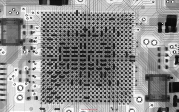
How to Repair PCB Assembly Issues
Once a defect is confirmed, repair is usually possible — as long as the damage is localized and the board hasn't been compromised structurally. Here's how the most common repairs are typically handled:
Reworking a Solder Joint
For a cold joint or insufficient solder, reflow the connection with a soldering iron, apply a small amount of flux, and add fresh solder until a smooth, concave fillet forms. This is usually enough to restore a reliable connection without removing the component.
Desoldering and Replacing a Component
For a damaged or incorrectly placed component, a hot air rework station is used to evenly heat the part until the existing solder melts, after which it can be lifted, the pads cleaned, and a replacement part soldered into place with careful attention to alignment.
Fixing Solder Bridges
A solder bridge can often be cleared with solder wick and a soldering iron, drawing the excess solder away from the pads until the short is removed.
Repairing Damaged Traces
Small breaks near a component can be bridged with a conductive pen or a thin jumper wire, with care taken to insulate the repair and avoid introducing a new short.
BGA Reballing
For BGA components with void or opens beneath the package, reballing — removing the part, cleaning the pads, and applying a fresh, properly reflowed set of solder balls — restores the hidden connections that can't be reached with a soldering iron.
Whatever the repair, work on an ESD-safe mat with a grounded wrist strap. A repair that fixes the original defect but introduces static damage to a nearby component isn't really a fix.
Preventing PCB Assembly Issues Before They Start
Repair and diagnosis are useful skills, but the boards that cause the fewest problems are the ones where issues were caught before assembly ever began. A few practices make the biggest difference:
1. Run a DFM check before production. Reviewing footprints, pad sizes, and clearances against manufacturability guidelines catches many of the issues in the table above before a single component is placed.
2. Match the reflow profile to every component on the board — not just the largest or most sensitive one — to avoid both cold joints and thermal damage.
3. Store and handle moisture-sensitive components correctly, and use ESD-safe practices throughout handling, not just during the repair stage.
4. Choose an assembly partner with more than one inspection checkpoint. AOI alone won't catch a void hidden under a BGA; X-ray inspection alone won't catch a bridge on a visible pad. The two together cover far more ground.
PCBgogo builds these checks into its standard assembly process — a DFM review ahead of production, AOI and X-ray inspection on finished boards, and electrical testing before shipment — which is generally where a well-run assembly service earns its keep: preventing the issues covered in this guide from reaching you in the first place, rather than leaving you to catch them after the fact.
Final Thoughts
Most PCB assembly issues are preventable, diagnosable, and — when caught early — repairable. The boards that cause the least trouble downstream are usually the ones that went through a DFM check before production and a layered inspection process before shipment, rather than relying on a single catch-all test at the end. If you're comparing assembly partners, ask specifically what inspection steps are included as standard, rather than assuming "tested before shipping" means the same thing everywhere.
Frequently Asked Questions
What are the most common PCB assembly issues?
Solder joint problems — cold joints, bridging, insufficient solder, and tombstoning — are the most frequent issues, followed by component placement errors and BOM or footprint mismatches. See the table above for a full breakdown by category.
Can PCB assembly issues be repaired without sending the board back?
Many localized issues — a cold joint, a misaligned component, a small trace break — can be repaired on the bench with basic rework tools. Widespread defects across a batch, or structural issues like warpage, are usually better handled by going back to the manufacturer.
How do manufacturers catch assembly defects before shipping?
Most use a layered approach: automated optical inspection (AOI) for surface-level defects, X-ray inspection for hidden joints under BGA and QFN packages, and electrical testing to confirm the board performs correctly.
Is a PCB assembly issue different from a PCB fabrication issue?
Yes. Fabrication issues originate in how the bare board itself is manufactured — copper etching, drilling, plating — while assembly issues occur when components are placed and soldered onto a board. A board can pass fabrication inspection cleanly and still develop issues during assembly, and vice versa.





