日本語
 한국어

PCB Antenna Design for Wireless Products
Effective PCB antenna design starts with the assembled device. Choose a layout for the band and board edge, copy the reference geometry and keepout, and route the feed for the chosen stackup. Then tune with the enclosure installed and verify range in the intended use; S11 alone cannot establish it.
A bare prototype can lose range after its battery and lid are fitted. The copper has not moved; its electrical surroundings have. This workflow catches those changes before production.
Start PCB Antenna Design With Product Constraints
Fix the band, board outline, enclosure, and nearby metal before drawing the antenna. On a 2.4 GHz Bluetooth sensor, the battery, charging connector, and user's hand determine which edge offers clear radiating space. Reserve it first. A later placement change needs another tuning pass.
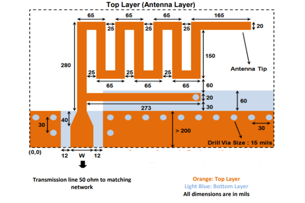
Choose the Antenna Around the Board
The first PCB antenna design decision is whether the radiator sits in copper, on a chip, or outside the enclosure. Compare the tradeoffs before reserving space.
| Option | Good fit | Watch for |
|---|---|---|
| PCB trace | Room at a clear board edge; low parts count | Ground size, keepout, and enclosure changes can shift tuning |
| Chip antenna | A compact board with a proven supplier layout | Still needs its specified clearance and final-product tuning |
| External | Metal housing or too little radiating space on the PCB | Connector, cable, placement, and assembly cost |
A printed trace can simplify PCB antenna design in a plastic sensor with a clear board edge. A metal enclosure may favor an external antenna.
Keep the Feed and Radiator Rules Separate
In PCB antenna design, the RF feed needs continuous ground, while the radiator needs the reference layout's specified clearance. Check both before sending Gerbers:
Copy the full reference. Preserve its shape, feed, board edge, keepouts, and ground dimensions. If stackup or outline changes, retest; copper alone is not the complete PCB antenna design.
Define the feed for the real stackup. Specify the 50 Ω trace using actual dielectric thickness and copper weight. Keep its return path continuous and avoid branches. Feed impedance is a PCB antenna design input, not proof of radiated performance.
Leave room to tune. Put matching footprints near the feed with short ground connections. Start with reference values; choose final parts after measurement.
Build a representative sample. Fit battery, shields, cables, fasteners, and housing before tuning. Use the reference's keepout rather than a generic clearance number.
For controlled-impedance PCB antenna design, send PCBgogo the target feed impedance, stackup, and Gerbers before fabrication. PCBgogo can confirm the stated manufacturing requirements; final tuning still happens in the product.
PCBgogo - Reliable, High-Quality PCB Manufacturing
PCBgogo is a one-stop PCB and PCBA manufacturing factory, helping you save time and costs while ensuring consistent, reliable quality.
Get a Free Quote >
Measure the Finished Product
PCB antenna design is not finished when a network analyzer shows a dip at center frequency. Calibrate at the feed, sweep the full band, and compare S11 with the housing open and closed. Below ?10 dB across the band is a useful matching target, not proof of efficiency or range.
In a Texas Instruments 2.4 GHz USB-dongle test, a plastic cover shifted resonance lower; connection to a laptop narrowed measured bandwidth from about 250 MHz to 100 MHz. Your product will differ, but the case shows why final surroundings belong in the test.
For PCB antenna design approval, run a repeatable link test at representative distances and orientations on several production-intent boards. If the lid shifts resonance, revise the trace or match, record the fitted parts and stackup, then retest. That record helps diagnose a later PCB antenna design revision.
What to Check Before Ordering
A final PCB antenna design review compares production files with the tested configuration:
Board outline, antenna copper, and every specified layer keepout match the approved revision.
Stackup, copper weight, and any controlled-impedance target are written in the fabrication notes.
The matching bill of materials lists fitted values, and test notes identify the enclosure and battery state.
Common PCB Antenna Design Questions
Can I copy a 2.4 GHz reference antenna onto my board?
Use its complete layout as a starting point, including ground, keepout, and stackup. Changing the board or enclosure changes the RF environment, so measure and retune the assembled device.
Does a 50 Ω feed guarantee good range?
No. It helps transfer power to the antenna, but poor placement or nearby metal can still reduce radiated performance. Check S11 and a repeatable real-world link test.
Good PCB antenna design keeps the same board, enclosure, and matching assumptions from prototype through production.