
 日本語
日本語
 한국어
한국어

PCB Outer Layer Circuit Manufacturing Guide
The PCB outer layer circuit carries both the component soldering pads and the external signal routing, so its precision directly determines trace width tolerance, impedance consistency, and overall board yield. Unlike inner layer circuits, which typically use a straightforward image transfer and etching subtractive process, outer layer circuits must simultaneously metallize plated through holes. For this reason, manufacturers generally rely on a negative pattern plating, etching, and tin stripping process. This article explains the complete outer layer manufacturing process, from imaging to etching and tin stripping, and shows how each step affects circuit precision, copper thickness, impedance, and production yield.
How Outer Layer Circuits Differ From Inner Layer Circuits
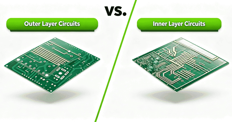
Inner layer circuits involve no plating before etching — the copper thickness is simply the base copper weight of the laminate, which keeps the process comparatively straightforward. Outer layers are different: because the hole walls need to carry current along the same conductive path as the surface traces, the outer layer image, once developed, must go through pattern plating first. This thickens both the trace copper and the hole-wall copper together, then adds a tin layer as an etch resist, and only afterward etches away the copper outside the circuit pattern and strips the tin. This "plate first, etch later" negative-image sequence is the defining feature that separates outer layer circuits from inner layers — and it's also why controlling copper thickness and trace width on outer layers is inherently more demanding.
Outer Layer Imaging Process, Step by Step
1. Outer Layer Dry Film Lamination / Wet Film Coating
Outer layer circuit fabrication starts with image transfer: a photosensitive dry film is laminated (or a wet film coated) onto the pre-treated copper-clad surface. Under heat and pressure, the dry film softens and conforms to both the copper surface and the hole walls. Lamination temperature, pressure, and feed speed together determine film thickness uniformity and hole-opening coverage, which directly affects the clarity of the exposed image downstream.
2. Outer Layer LDI Direct Imaging vs. Film Exposure
Exposure is the step that most directly determines circuit precision. Traditional film exposure requires generating a photo-tool first, then aligning it to the substrate for exposure — a process prone to registration error from film expansion and contraction. LDI (Laser Direct Imaging) eliminates the photo-tool step entirely: a laser head scans the circuit pattern directly onto the dry film, delivering higher registration accuracy and finer trace capability.
| Exposure Method | Image Source | Registration Method | Best Suited For |
|---|---|---|---|
| Film exposure | Photo-tool film | Manual / mechanical registration | Standard trace width and spacing |
| LDI direct imaging | Digital pattern, scanned directly | Automated optical registration | Fine-line, high-density, HDI circuits |
3. Outer Layer Developing
After exposure, the board is rinsed with a developer solution that dissolves the unpolymerized dry film, leaving the cured, polymerized film in place as the plating window. Developing time, developer concentration, and feed speed must be tightly controlled — under-developing leaves residual film that interferes with plating, while over-developing can distort the circuit pattern.
Pattern Plating: The Core Step That Forms the Outer Layer Circuit
Once developing is complete, the exposed copper — including the hole walls — enters pattern plating, the most technically demanding step in the outer layer process. It consists of two parts:
Copper thickening: electroplating deposits additional copper onto the circuit windows and hole walls, bringing hole copper thickness up to the level needed for conductivity and current-carrying capacity while improving trace copper thickness uniformity. Uneven copper thickness directly affects etching consistency later on, which in turn causes trace width deviation.
Tin plating as etch resist: after copper plating, a layer of tin is plated on top to serve as the etch resist, protecting both the trace copper and the hole-wall copper during the subsequent etching step. Unlike inner layers, which rely on the dry film itself as the etch resist, outer layers use a metallic tin layer — offering stronger etch resistance and better protection for hole-wall copper.
Etching + Tin Stripping: Forming the Outer Layer Circuit Through the Negative Process
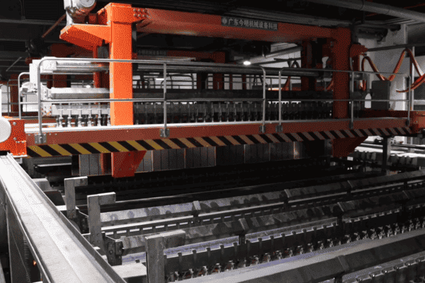
After pattern plating, the surface dry film is stripped away, exposing the bare copper areas that were never protected by tin. The board then enters etching. The etchant dissolves the copper that isn't protected by tin, leaving only the trace copper and hole copper under the tin layer — this is how the negative-image process forms the final outer layer circuit pattern. Etching time, temperature, and chemical concentration must be precisely matched to copper thickness: under-etching leaves residual copper that risks short circuits, while over-etching causes undercut, narrowing trace width and pushing impedance away from the design target. Once etching is complete, a tin-stripping step removes the surface tin layer, revealing the final copper trace and completing the outer layer circuit.
Key Factors That Affect Outer Layer Circuit Precision and Yield
| Factor | Common Impact | Control Point |
|---|---|---|
| Exposure equipment precision | Trace width/spacing deviation, poor registration | Prioritize LDI with automated optical registration |
| Plated copper thickness uniformity | Impedance inconsistency, thin hole copper | Control current distribution via plating parameters and rack/fixture design |
| Etch factor control | Undercut narrows trace width | Precisely control etch time, temperature, and chemical concentration |
| Inspection | Residual copper, shorts, and opens go undetected | AOI inspection after etching, compared against the Gerber design |
PCBgogo's Capabilities in Outer Layer Circuit Production
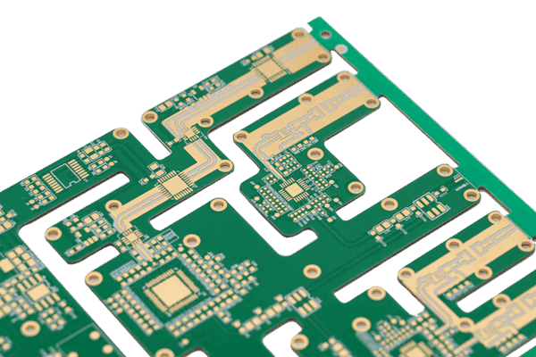
Circuit consistency after etching and tin stripping ultimately still needs to be verified through inspection. PCBgogo uses AOI (Automated Optical Inspection) as a standard inspection step in its production process, comparing the etched circuit pattern against the design Gerber file. PCBgogo also has HDI fine-line manufacturing capability and offers a free DFM check for customers, helping catch trace width/spacing manufacturability risks before an order is placed.
Frequently Asked Questions
Does every outer layer circuit require pattern plating?
Yes. Because outer layer circuits need the hole-wall copper thickened at the same time as the surface traces to ensure hole conductivity and current-carrying capacity, pattern plating is the standard approach — and it's one of the key differences between outer and inner layer processes.
How much more precise is LDI exposure compared to film exposure?
LDI eliminates the photo-tool generation and registration steps, avoiding the alignment errors caused by film expansion and contraction from heat. For fine-line, high-density designs, it generally delivers better registration accuracy and trace width consistency, though whether it's necessary depends on the specific trace width and spacing requirements.
How does etching affect impedance?
Undercut during etching makes the actual trace width narrower than the design width. That width deviation directly changes the trace's characteristic impedance, which is why stable control of the etch factor and chemical concentration matters most for high-speed signal boards.
Conclusion
The outer layer process spans three major stages — image transfer, pattern plating, and etching with tin stripping — and each step compounds its effect on final circuit precision and yield. Understanding this "plate first, etch later" negative-image logic helps engineers build in reasonable manufacturability margin at the design stage.





