




 日本語
日本語
 한국어
한국어

How Does a Low Profile Keyboard PCB Improve Thin Designs
QUICK ANSWER A low-profile keyboard uses shorter switches and keycaps, but the PCB determines whether the thin structure is reliable. The board must hold switch geometry, stabilize hot-swap sockets or solder joints, route the key matrix, protect USB and wireless circuits, and remain flat enough for consistent key feel across the assembly.
Key Takeaways
Mechanical stack first: Choose the switch, socket, stabilizer, plate, PCB thickness, and case datum before routing.
Footprints are ecosystem-specific: Verify the exact supplier drawing because low-profile sockets and full-height sockets usually differ.
Flatness affects feel: Board bow can change switch seating, keycap height, and solder joint stress.
Routing must remain serviceable: Keep the matrix simple and preserve test points for rows, columns, power, and data.
Prototype the full stack: The decisive build includes the plate, switches, sockets, stabilizers, keycaps, enclosure, and firmware.
Introduction
A thin keyboard can look simple from the outside, yet a difference of a fraction of a millimeter can decide whether every switch sits evenly or the finished product feels inconsistent. The PCB is the mechanical reference for the switch field as well as the electrical platform for the matrix, controller, lighting, USB, battery, and wireless functions.
This guide explains what makes a low profile keyboard different, which PCB processes deserve extra attention, how to prepare production files, and what to test before moving from prototypes to a repeatable build.
What Is a Low Profile Keyboard
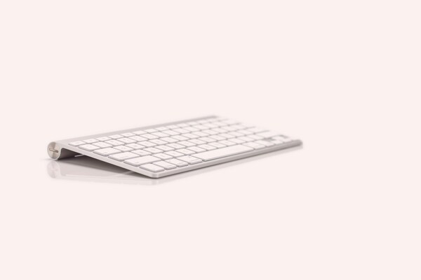
A low-profile keyboard is a keyboard built around switches, keycaps, and an enclosure stack that is shorter than a conventional mechanical keyboard. The term describes the complete mechanical system, not a universal switch standard, so two low-profile families may use different pins, sockets, stabilizers, cap mounts, and plate openings.
The PCB usually carries a row and column matrix scanned by a microcontroller. A diode at each key can block unintended current paths during simultaneous presses. A common full-size grid uses 19.05 mm center spacing, but compact layouts and special keys can change local geometry. The supplier drawing should control every pad and cutout.
Low height also changes the tolerance stack. PCB thickness, socket body, plate, foam, case bosses, and keycap clearance all accumulate. Closing the stack before measuring real parts can bend the board, overcompress foam, or leave switches partly unseated.
How Does a Low Profile Keyboard PCB Differ From a Standard Keyboard PCB
A low-profile keyboard PCB carries many familiar keyboard circuits, but it has less vertical room and less tolerance for footprint or flatness errors. The practical differences appear where mechanics, assembly, and routing meet.
Switch mounting: Through-hole contacts and SMT hot-swap sockets require different land patterns. Match the PCB, plate opening, and retention method to the exact series.
Stabilizer geometry: Check wide key travel so the wire, socket, LED, and nearby parts cannot collide.
Component height: Keep tall parts away from the plate and case ribs. Use a height map for both PCB sides.
Board support: Use enough mounting points to resist flex during typing and switch insertion without crushing parts or distorting the matrix area.
Integrated functions: Wireless, RGB, displays, and charging can justify a four-layer design with stronger return path and power planning.
These differences do not automatically require advanced fabrication, but they make early stack review and disciplined file preparation much more valuable.
What Special Manufacturing Processes Does a Low Profile Keyboard Need
The special manufacturing work is mainly tight mechanical registration, controlled board geometry, suitable surface finish, and assembly processes matched to small sockets and mixed component heights. The table connects each process choice to the defect it is meant to prevent.
| Process choice | Why it matters | Practical design action |
|---|---|---|
| Thickness and flatness control | The PCB is part of the switch stack and influences seating across the key field. | State finished thickness and tolerance. Balance copper across the board. |
| Accurate routing and drilling | Switch pins, stabilizer openings, mounting holes, and case features must share one coordinate system. | Dimension critical holes from fixed datums and confirm plated versus nonplated status. |
| Solder mask registration | Fine socket and LED pads leave little room for mask encroachment. | Use the assembler's rules and review narrow mask webs during DFM. |
| Planar surface finish | SMT sockets, small passives, and fine pitch controllers need consistent paste transfer and joint formation. | Choose a finish that suits the pad geometry, storage plan, and assembly profile. |
| SMT and through-hole sequencing | A board may combine sockets, LEDs, USB connectors, switches, and encoders. | Mark polarity and agree on reflow and secondary soldering steps. |
Controlled impedance matters for USB differential data and other high-speed interfaces. USB 2.0 commonly targets a 90-ohm differential pair, but trace geometry must come from the approved stackup. Keep a continuous reference plane, minimize stubs, and place ESD protection close to the connector.
How Should You Design the PCB Before Requesting a Quote
A quote becomes accurate when the design package defines the mechanical stack, electrical requirements, assembly scope, and inspection expectations without forcing the manufacturer to guess. A reliable workflow follows the order below.
Freeze the switch ecosystem: Record exact switch, socket, keycap, stabilizer, plate, and connector part numbers. Verify controlled footprints against a one-to-one print or mechanical model.
Build the key grid from datums: Place switch centers, stabilizer holes, and plate openings from one origin, then lock them before routing.
Calculate the height chain: List dimensions and tolerances for the case, standoffs, PCB, socket, switch, plate, foam, and keycap at full travel.
Plan the matrix and rollover: Assign rows and columns to reduce crossings, add key diodes where required, and use net names that match the test plan.
Protect power and interfaces: Place decoupling near IC supply pins, preserve return paths, and separate LED current loops from reset, crystal, antenna, and data circuits.
Design for assembly and test: Add fiducials, polarity marks, probe access, and tooling clearance. Keep test pads clear of sockets, stabilizers, ribs, coating, and foam.
For wireless versions, treat the antenna area as both a mechanical and copper keepout. Test radio performance with the final enclosure, battery, plate, and cable installed.
How PCBgogo Supports Complex Low Profile Keyboard Manufacturing
Complexity rises when a low-profile keyboard combines thin mechanics with dense routing, wireless functions, lighting, fine pitch controllers, flex connections, or mixed assembly. PCBgogo can support that transition through verified fabrication, assembly, review, and inspection capabilities.
Fabrication options: PCBgogo manufactures rigid, flexible, and rigid-flex boards and can review HDI, blind or buried vias, via-in-pad, controlled impedance, and several surface finishes.
Mixed assembly: Its assembly service supports SMT, through-hole, and mixed technology builds, which suits keyboards that combine small passives and controllers with connectors, encoders, or switch hardware.
DFM review: Engineering review can identify fabrication, assembly, panelization, and test access conflicts before material is committed. Supplying the stack drawing and component height limits makes that review more useful.
Inspection and electrical test: Available processes include automated optical inspection, X-ray inspection, flying probe testing, and fixture-based testing. Select them by package type, volume, and required coverage.
Prototype through production: Prototype and volume assembly are available within the same service scope, allowing approved files, substitutions, process notes, and inspection criteria to remain controlled as quantities increase.
Submit fabrication and assembly data together, then resolve DFM questions before freezing the production revision. Use advanced processes only for a defined density, signal, or mechanical need.
PCBgogo - Reliable, High-Quality PCB Manufacturing
Save time and money with an all-in-one solution for PCB fabrication, assembly, and parts. Reduce vendor coordination, avoid split shipments, and get consistent, reliable quality.
Get Free Quote >
What Should Be Included in the Manufacturing Package
A complete manufacturing package tells the fabricator what to build and tells the assembler how to populate, inspect, and test it. Keep every file on the same revision and include the following items.
| File or note | Required content | Keyboard-specific check |
|---|---|---|
| Fabrication data | Gerber or ODB data, drill files, outline, stackup, copper weight, finish, thickness, and controlled impedance notes | Separate plated and nonplated switch, stabilizer, and mounting holes. |
| Assembly data | BOM, centroid file, assembly drawings, polarity, do not fit list, and approved substitutions | Identify the exact low-profile socket and switch family. Do not use a generic description. |
| Mechanical data | Dimensioned drawing and, when possible, a STEP model of the full assembly | Show plate datum, connector opening, keycap envelope, stabilizer travel, and case keepouts. |
| Test requirements | Bare board net test, PCBA inspection, programming, and functional test instructions | Provide a matrix test map, USB or wireless check, LED pattern, and current limit. |
IPC 2221 covers general design, IPC 6012 addresses rigid board qualification, IPC A 600 covers bare board acceptability, and IPC A 610 covers assembly acceptability. The purchase package must still state the required class, exceptions, test coverage, and product-specific limits.
How Do You Validate a Prototype Before Production
Prototype validation should prove mechanical fit, electrical behavior, firmware function, and assembly repeatability before the revision is released. Test at least several completed units so a single damaged board is not mistaken for a design trend.
Mechanical fit: Assemble all production-intent parts. Check switch seating, keycap gaps, stabilizer return, connector access, screw torque, and case closure.
Matrix coverage: Exercise every key alone and across shared rows and columns. Check for missing, stuck, ghost, or swapped keys.
Interface behavior: Repeat USB insertion, enumeration, wake, suspend, and reconnect tests. For wireless models, test pairing and range in the final enclosure.
Lighting and power: Run maximum intended brightness with demanding key activity. Measure current, regulator temperature, charging behavior, and voltage at distant LEDs.
Physical stress: Cycle hot-swap switches, inspect socket joints, and watch for PCB flex. Recheck operation after transport and planned environmental exposure.
Record failures by unit, location, and revision. A production release should link the approved Gerber data, BOM, centroid file, firmware, fixture program, and inspection criteria to one controlled version.
Frequently Asked Questions About Low Profile Keyboard PCBs
Can a low profile keyboard use a standard mechanical keyboard PCB
Usually no. Low profile switch pins, sockets, stabilizers, plate openings, and keycap geometry often differ from full height systems. A standard PCB is usable only when every mechanical and electrical interface is explicitly compatible.
Should the PCB be two layers or four layers
A wired matrix with modest lighting can often be routed on two layers, while a wireless design or a board with dense RGB, USB, charging, and display circuits may benefit from four layers. Choose the layer count from routing density, return paths, emissions risk, and assembly cost rather than keyboard size alone.
Is hot swap more difficult to manufacture than soldered switches
Hot swap assembly adds footprint, paste, socket orientation, and mechanical load concerns. The socket solder joints must survive switch insertion and removal, so pad geometry, stencil apertures, board support, and inspection deserve early review.
Does every key need a diode
A diode per key is the common approach when reliable detection of multiple simultaneous keys is required. Designs with limited rollover can use other matrix strategies, but firmware behavior and ghosting must be tested against the actual user scenarios.
What is the most useful first prototype?
The most useful first prototype is a fully assembled keyboard stack, not only a powered bare PCB. It should include production-intent switches, sockets, plate, stabilizers, keycaps, enclosure parts, connectors, battery, and firmware so electrical and mechanical faults can be separated.
Conclusion
A reliable low-profile keyboard begins with a controlled mechanical stack and a PCB that translates that geometry into manufacturable copper, holes, pads, assembly access, and test coverage. Freeze the switch ecosystem first, design from shared datums, submit a complete data package, and validate several full assemblies before production. Those steps protect the thin form factor without trading away key feel, serviceability, or electrical reliability.





