



 日本語
日本語
 한국어
한국어

Laser Engraving a PCB Board
Laser engraving a PCB board means using a laser to burn away a resist coating on a copper-clad board, which is then chemically etched to form circuit traces. It works for single-sided prototypes with traces around 0.2mm, but it cannot plate vias, build multilayer stacks, or add soldermask, which is why most designs eventually move to professional fabrication.
The first time I watched a coworker spray a copper board matte black, run it under a diode laser, then drop it into a tray of etchant, it looked like a magic trick. Twenty minutes later, he had a working prototype, no order placed, no shipping wait, just a board he had burned into existence at his own bench.
That trick has limits, and this article walks through what laser engraving actually does to a PCB, where it holds up, where it falls apart, and how to tell when it is time to send the design to a fab instead.
What Actually Happens When You Laser Engrave a PCB
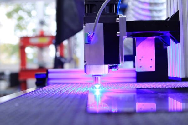
Laser engraving a PCB board does not cut copper directly. It removes a protective layer, usually black paint or a UV-sensitive film, so that an acid bath can dissolve the exposed copper underneath. The laser plays the role that a printed film mask and UV exposure play in a standard photoresist process, just without the darkroom.
Three laser families show up in home and small shop setups, each suited to a different part of the job.
CO2 lasers (10.6 micron infrared): common in desktop laser cutters and effective at burning through spray paint mask in a few low power passes, but copper reflects most of the infrared energy so the laser never touches the metal directly.
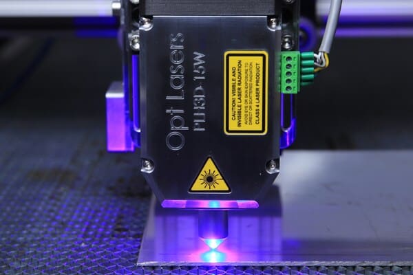
Diode and blue or UV lasers (400 to 450 nanometers): shorter wavelengths absorb into copper and paint more readily, which is why hobbyists mount small 405nm or 445nm diode modules on CNC frames or repurposed 3D printers for finer trace work.
Fiber and UV industrial lasers (1064nm and 355nm): the tools behind true industrial laser etching lines, capable of ablating copper directly without a mask, but the equipment cost puts them well outside typical hobby budgets.
Once the mask is cleared, the actual trace quality comes down to how the laser is dialed in, not just which laser you own.
Where Laser Engraved PCBs Genuinely Work Well
A laser-engraved board earns its keep in low-stakes, short-lived, single-sided projects where speed matters more than polish.
Brushless motor driver boards: quick functional prototypes for testing a control loop before committing to a production layout.
Arduino shields and sensor breakouts: simple footprints with generous trace widths that tolerate the resolution limits of a home laser.
Custom SMT stencils: laser-cut stencils for solder paste, a task that plays to a laser's strength since it is cutting through thin material rather than patterning copper.
Classroom and workshop demonstrations: a fast way to show students the relationship between a Gerber layout and a physical board without waiting on shipping.
These use cases share one thing in common: they can tolerate a rough edge. Anything closer to a shipped product runs into the next set of problems fast.
Where a Home Laser Setup Runs Into Trouble
The gap between a laser-engraved prototype and a manufacturable board comes down to five recurring failure points.
Trace resolution: a typical desktop laser spot lands around 0.2 to 0.5mm, which rules out fine-pitch parts and dense digital layouts from the start.
Unplated vias: holes drilled by hand have no copper plating on the barrel, so layer-to-layer connections rely on soldered wire jumpers instead of a real plated through hole.
No multilayer buildup: there is no way to laminate and align multiple patterned inner layers at home, so any design needing buried planes or blind vias is off the table entirely.
No protective finish: bare copper left exposed after etching oxidizes over time, and DIY workarounds like clear nail polish are not a substitute for soldermask or a real surface finish.
Panel level inconsistency: any tilt in the board or drift in laser focus shows up as uneven mask removal across a larger panel, something a fixed industrial process controls for by design.
These are not edge cases; they are the default outcome once a design grows past a single quick prototype, which is why most PCB designers eventually compare the two approaches side by side.
The table below lines up laser-engraved boards against professionally fabricated boards on the factors that matter most once a design leaves the prototype stage.
| Factor | Laser Engraved (DIY) | Professional Fabrication |
|---|---|---|
| Minimum trace and space | Roughly 0.2 to 0.5mm | Commonly around 0.1mm (4 mil) on standard builds |
| Via plating | None, holes are unplated | Drilled and copper plated automatically |
| Layer count | Single sided, occasionally basic double sided | Two layers up through advanced multilayer stacks |
| Protective finish | Bare copper, no soldermask | Soldermask plus a chosen surface finish |
| Panel consistency | Varies with focus and board flatness | Controlled uniformly across the full panel |
| Best fit | One-off prototypes, stencils, teaching boards | Repeatable, reliable, production-ready boards |
Why Standards Exist Beyond a Single Certification
Professional PCB fabrication is not judged by one badge on a datasheet; it is judged by a stack of process controls that each cover a different failure mode.
ISO 9001: governs the quality management system behind how a factory documents and repeats its processes, not the board itself.
IATF 16949: an automotive-specific quality standard that adds traceability and defect prevention requirements on top of ISO 9001.
RoHS: restricts hazardous substances like lead and certain flame retardants in the materials used to build the board.
UL certification: verifies that base materials meet defined flammability and safety ratings.
IPC design standards: the industry reference point that most fabricators build their minimum trace, space, and hole size rules around, which is part of why professional boards land in a tighter, more predictable tolerance band than a hand-built one.
None of these standards guarantee a board works for your specific application; they guarantee the process that built it was controlled and repeatable, which is exactly the piece a laser and an etch tank at home cannot offer.
When It Is Time to Order Instead of Etch
The decision point usually shows up the moment a design needs more than one identical board, a plated via, or a layer count above one.
This is where a manufacturing partner with real process control picks up where a home laser leaves off. PCBgogo sources its laminates from established suppliers like Shengyi and Kingboard, and fabricates boards up to 40 layers, including blind and buried vias and laser-drilled microvias, none of which a desktop laser setup can replicate at any resolution. Every order goes through automated optical inspection and X-ray inspection along with a per-order DFM and engineer review, catching the exact kind of undercut, misalignment, and incomplete etch issues that plague a hand-built board. For designs that need to move fast, PCBgogo offers expedited delivery options, and native file support for Eagle, Altium, and PADS means a layout can go from design software straight to production without a manual export step. If a project has reached the point where it needs plated vias, a real surface finish, or more than a handful of identical boards, the PCBgogo online quoting tool is the faster and more reliable next step.
Safety Cannot Be an Afterthought
Burning through FR4 or a paint mask releases fumes that are genuinely hazardous, not just unpleasant.
Stanford's laser cutter safety guidance groups these into three risk categories: fire hazard from unsuitable substrate materials or insufficient exhaust ventilation, respiratory hazard from the fumes and particulates generated as material is burned or vaporized, and direct laser hazard from Class 3B and Class 4 beams, which is why ANSI Z136.1 exists as the safe use of lasers standard that most institutional laser labs are built around. In practice, that means running any laser work on copper-clad board under local exhaust ventilation, not just an open window, and never leaving the machine unattended while it is cutting.
Conclusion
Laser engraving earns its place as a fast, low-cost way to test a simple layout before committing to anything bigger. The moment a design needs plated vias, multiple layers, or more than a couple of identical boards, that same speed becomes a liability, and a manufacturing partner built for repeatable, inspected production is the more direct path from finished Gerber file to working board.
Frequently Asked Questions
Can a laser cutter make a full PCB without any chemical etching?
Not in most home setups. A hobby laser typically removes a resist or paint mask, and the copper still needs a chemical etch bath afterward. True direct copper ablation without etching requires industrial-grade fiber or UV lasers.
What is the finest trace a DIY laser-engraved PCB can achieve?
Around 0.2mm in practice, depending on the laser and focus quality. Designs that need 0.1mm traces or finer pitch components need professional fabrication.
Can laser engraved PCBs have plated vias?
No. Holes drilled after laser etching are unplated, so connections between sides typically rely on soldered wire jumpers rather than a true plated through hole.
Is laser engraving a PCB at home safe?
It can be done safely with the right precautions, including laser safety glasses, local exhaust ventilation, and never leaving the machine unattended. Burning FR4 or paint mask releases fumes that need proper extraction, not just an open window.
How many identical boards can I laser engrave in a reasonable amount of time?
Realistically, only a handful. A single small board can take 10 to 20 minutes to engrave plus a separate etch cycle, so batches of 10 or more quickly become impractical compared to a fabricator producing them in parallel.
When should I switch from laser engraving to professional PCB fabrication?
Once a design needs multiple identical boards, plated vias, more than one copper layer, or fine-pitch components, professional fabrication becomes faster and more reliable than continuing to etch boards by hand.





