
 日本語
日本語
 한국어
한국어

Industrial PCB Production Process and Quality Guide
Industrial PCB production converts released design files into repeatable circuit boards through CAM review, imaging, etching, lamination, drilling, plating, finishing, and electrical test. Compared with prototyping, production requires tighter change control, stable materials, panel planning, process traceability, and acceptance criteria that can be applied consistently across every lot.
Why Industrial PCB Production Needs a Controlled Process
Industrial PCB production is a controlled manufacturing system built to reproduce the same electrical and mechanical result across a batch. A prototype only has to prove that a circuit can work. A production release must also prove that the board can be fabricated, assembled, inspected, and tested without relying on hand fixes or undocumented judgment.
A single multilayer board passes through dozens of linked operations, from preproduction engineering and CAM review through imaging, etching, lamination, drilling, plating, and final routing. An error found after lamination or plating costs more to correct than the same error found during CAM review, which is why production engineering begins before material reaches the line.
The sections below follow the decisions a buyer or hardware team must make before volume rises. The process starts with the product environment, then moves through materials, fabrication controls, inspection, and the data package that keeps repeat orders consistent.
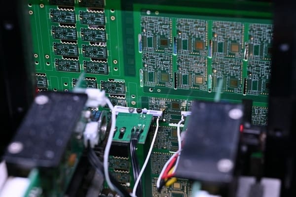
Where Industrial PCBs Are Used
Industrial PCB applications are products that need repeatable performance under defined electrical, thermal, mechanical, or service conditions. The product environment determines the board construction and inspection plan more reliably than the word industrial by itself.
Motor drives: Variable frequency drives and servo controllers carry switching current and generate heat. Designers often need heavier copper, short power loops, suitable creepage, and a thermal path that keeps gate drivers and current sensors within rating.
Programmable logic controllers: PLC input and output modules combine field wiring, isolation, digital logic, and communication interfaces. Stable connector geometry and clear separation between field and logic domains matter during both fabrication and assembly.
Industrial sensor transmitters: Pressure, temperature, flow, and vibration transmitters often process millivolt level signals beside digital communication. Clean grounding and controlled analog routing protect measurement accuracy.
Power conversion modules: AC input supplies and DC converters combine high voltage, high current, magnetics, and heat. Material temperature rating and spacing must be set from the actual safety and operating requirements.
These examples show why a production plan begins with use conditions. The same schematic can need a different stackup, finish, copper weight, or test strategy when the enclosure, voltage, or expected service life changes.
How the Industrial PCB Manufacturing Process Works
The industrial PCB manufacturing process transforms approved digital data into copper features, plated interconnections, protected surfaces, and a verified netlist. Each stage creates an output that becomes the input to the next stage, so inspection is placed before defects become buried or expensive.
This table shows the core production stages and the control that protects yield at each point.
| Stage | What happens | Primary control |
|---|---|---|
| CAM review | Gerber, drill, netlist, outline, and stackup data are checked and converted into tooling. | DFM rules and file revision check |
| Inner imaging | Photoresist is exposed and developed to define copper on each inner core. | Registration targets and AOI |
| Etching | Unwanted copper is removed and the remaining circuit is cleaned. | Chemistry, spray pressure, and line speed |
| Lamination | Cores, prepreg, and copper foil are bonded with heat and pressure. | Layup verification and press profile |
| Drilling and plating | Holes are drilled, desmeared, seeded, and plated to connect layers. | Tool wear, hole position, and microsection |
| Outer finish | Outer copper, solder mask, legend, and surface finish are completed. | Mask registration and finish inspection |
| Final test | Open and short testing is followed by dimensional and visual inspection. | Netlist test and shipment release |
Materials and Equipment That Shape Production Results
PCB materials and equipment shape production results because they set the electrical, thermal, and dimensional limits of the board. FR4 covers many industrial products, while high temperature laminate, metal core material, or high frequency laminate may be needed when heat or dielectric behavior dominates the design.
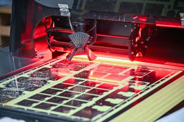
Laser direct imaging improves image registration for fine features. CNC drilling controls hole location, and plating lines build copper through the hole wall. AOI compares etched layers with design data.
X ray registration tools and microsection analysis reveal conditions that a surface camera cannot see. Equipment capability matters only when calibration, chemistry, and maintenance remain under control.
Quality Standards Used for Industrial PCB Production
Industrial PCB quality standards form a stack of design, performance, acceptability, and test requirements. They do not act as one universal certificate, and the purchase order must identify the documents and class that apply to the finished board.
IPC 6012: This specification defines qualification and performance requirements for rigid printed boards. IPC states that it covers single sided, double sided, multilayer, embedded circuitry, and metal core rigid constructions.
IPC A 600: This acceptability standard illustrates target, acceptable, and nonconforming conditions that can be observed externally or internally on bare boards.
IPC 9252: This document addresses electrical testing of unpopulated printed boards and supports a defined approach to continuity and isolation checks.
J STD 001 and IPC A 610: These apply after components are assembled. J STD 001 addresses soldered assembly process requirements, while IPC A 610 addresses postassembly acceptability.
A standard defines how evidence is judged, but it does not replace a complete drawing or customer specification. Controlled impedance, coupon reporting, special cleanliness limits, and serialization still need explicit order requirements.
What Determines Production Readiness
Production readiness is determined by file control, process margin, material availability, panel efficiency, and a testable acceptance plan. A working prototype is only one part of that decision.
Released manufacturing data: Use one approved revision of the Gerbers or ODB data, drill files, netlist, fabrication drawing, and stackup. File names and drawing notes must agree.
Manufacturing margin: Review annular rings, solder mask dams, copper to edge distance, hole aspect ratio, and routing tolerances against the selected factory process.
Material control: Name the required laminate, copper, finish, and approved equivalents. Confirm that impedance calculations use the production stackup.
Inspection and records: Define electrical test, sampling, microsection, dimensional reports, serialization, and any certificate required with shipment.
At this decision point, PCBgogo can connect DFM review, PCB fabrication, and assembly under one released data package. Its published capabilities include prototype through volume production, electrical testing, and ISO 9001 and IATF 16949 quality system compliance, which are relevant when a team needs repeatable builds rather than another informal sample.
PCBgogo - Reliable, High-Quality PCB Manufacturing
Save time and money with an all-in-one solution for PCB fabrication, assembly, and parts. Reduce vendor coordination, avoid split shipments, and get consistent, reliable quality.
Get Free Quote >
Yield Risks and Production Trends
The central production tension is higher circuit density with less tolerance for process variation. Yield falls when several borderline features occur on the same panel, even if each feature appears acceptable in isolation.
Fine geometry: Narrow traces, small annular rings, and tight mask dams reduce alignment and etching margin. DFM should identify the combined risk before tooling.
Advanced interconnects: Blind vias, buried vias, and microvias improve routing density but add sequential processing and inspection steps. Reliability depends on the approved construction.
Thermal stress: High power components and repeated temperature cycling expose weak plating, laminate, and solder joints. Thermal design must include the board and assembly together.
The practical response is to widen process margin where possible and collect evidence where margin cannot be widened. That balance protects both unit cost and field reliability.
Conclusion
Industrial PCB production succeeds when design data, material choices, process limits, and inspection criteria describe one repeatable product. Freeze the release, review it against the actual factory process, and use the pilot build to close risks before volume increases.
Frequently Asked Questions About Industrial PCB Production
These questions address the production decisions engineers and buyers most often need to settle before releasing a batch.
How is industrial PCB production different from prototyping?
Industrial PCB production prioritizes repeatability, traceability, stable materials, and controlled inspection across a batch. Prototyping prioritizes design learning and fast revision, often with fewer units and less dedicated tooling.
When should a PCB move into a pilot run?
A PCB should enter a pilot run after the circuit, stackup, BOM, and manufacturing files are frozen. The pilot should use the intended production process so its yield and test data are meaningful.
Which files are required for industrial PCB manufacturing?
A complete release normally includes Gerber or another supported fabrication dataset, NC drill files, a fabrication drawing, netlist, stackup, and readme notes. Assembly adds the BOM, centroid data, assembly drawings, and test instructions.
Does electrical testing prove that a PCB will function?
No. Bare board electrical testing checks opens and shorts against the netlist. Functional testing verifies the behavior of the assembled circuit under defined inputs and operating conditions.





