
 日本語
日本語
 한국어
한국어

AI Server PCB Guide: Layers, Materials, and Design Requirements
KEY DEFINITION An AI server PCB is a high-layer-count printed circuit board, typically 16 to 40 or more layers, engineered to route GPU accelerators, HBM memory, and NVLink or PCIe interconnects at multi-gigabit speeds. It requires low-loss laminates, HDI microvias, and heavy copper power planes to handle signal integrity and thermal loads that standard server boards were never built to manage.
A server built five years ago and a server built for AI training share a chassis size but almost nothing else underneath. Inside the AI version, the board itself has to survive current levels and data rates that would have been unthinkable on a standard rack server just a few years ago.
This guide breaks down what actually makes an AI server PCB different, from board types and materials to the design factors and quality checks that decide whether a board survives production.
Where AI Server PCB Design Actually Differs by Deployment
Not every AI server board faces the same constraints, because the workload, form factor, and layer budget change depending on where the server sits in the deployment stack.
Hyperscale training clusters: Rack systems built for distributed training pair eight or more GPUs per node with 24 to 40-plus layer baseboards and NVLink switch boards, using laminates rated for well over 100 Gb/s per lane.
Inference-optimized servers: Production servers running trained models spend less time on GPU-to-GPU bandwidth and more on PCIe host connectivity and network throughput, so layer counts often land at 16 to 24 instead of 32-plus.
Edge AI appliances: Compact inference boxes deployed in factories, retail sites, or telecom cabinets pack a single accelerator card into a smaller footprint, trading layer count for tighter thermal and space limits.
On-premise AI workstations: Enterprises running smaller models in-house use workstation-class boards with two to four GPUs, closer in complexity to a high-end desktop motherboard than a hyperscale baseboard.
Rack-scale liquid-cooled systems: Platforms that connect dozens of GPUs through a shared switch fabric must integrate cold plate mounting points directly into the board layout, not bolt them on afterward.
Regardless of the deployment, the boards inside an AI server fall into a handful of distinct PCB types, each with its own design profile.
The PCB Types Inside an AI Server
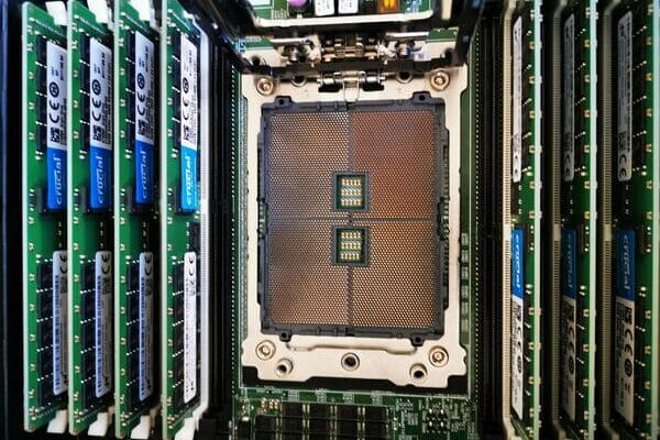
An AI server is not one board but several, and each type is built to a different layer count, material spec, and function.
The GPU baseboard hosts the accelerator modules and routes GPU-to-GPU interconnect traffic; in high-end platforms it commonly runs 24 to 40-plus layers using ultra-low-loss laminate to support NVLink-class signaling. The server motherboard handles the CPU, system memory, and PCIe switching at a comparatively modest 12 to 20 layers, since it carries less raw bandwidth than the GPU side.
| PCB Type | Typical Layer Count | Material Class | Primary Function |
|---|---|---|---|
| GPU baseboard | 24–40+ | Ultra-low-loss laminate | Mounts GPU modules, routes GPU interconnect |
| Server motherboard | 12–20 | Low-loss laminate | Hosts CPU, DDR5 memory, PCIe switching |
| Switch board | 32–40+ | Ultra-low-loss laminate | Routes interconnect traffic between GPUs |
| Network interface card | 12–18 | Low-loss laminate | High-speed cluster networking |
| Power distribution board | 4–12 | Heavy copper, high-Tg FR4 | Converts and distributes DC bus power |
Layer count and material choice are not arbitrary decisions made once and forgotten. They follow directly from a handful of design factors that apply across every board in the system.
What Actually Drives AI Server PCB Design Decisions
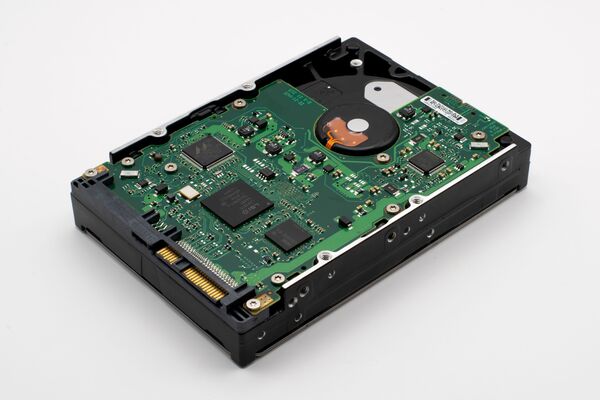
Several factors decide how an AI server PCB gets designed, and getting any one of them wrong shows up as signal loss, voltage droop, or a board that overheats under sustained load.
Signal integrity at high SerDes rates: Modern GPU interconnects and PCIe Gen5 links push tens of gigabits per second per lane, so dielectric loss, via stubs, and differential pair skew all have to stay within tight tolerances or the eye diagram closes.
Power delivery network design: A single GPU can draw 700 to 1,000-plus watts, so the board needs multi-phase voltage regulators placed close to the package and tiered decoupling capacitance to prevent voltage droop during compute bursts.
Layer count and HDI structure: Fine-pitch BGA packages with sub-0.5 mm ball pitch force the use of HDI microvias and sequential lamination, which is why GPU baseboards commonly run 24 to 40-plus layers compared to 8 to 12 on a conventional server board.
Thermal management at the board level: Sustained operation above 700 W per GPU requires dense thermal via arrays and, on some designs, copper coin inserts embedded directly under the GPU package to move heat into the cooling structure.
Material selection: Standard FR4 is too lossy for multi-gigabit signaling, so designers reserve low-loss or ultra-low-loss laminate for the critical routing layers and use FR4 only where speed requirements allow it.
Getting these factors right on paper is only half the job. Whether the board survives fabrication as designed comes down to the certification and inspection standards behind the manufacturing process.
The Certification and Inspection Stack Behind a Reliable AI Server PCB
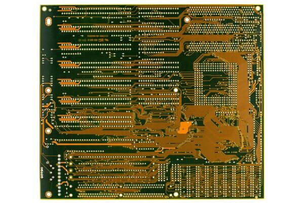
Certifications and inspection standards for AI server PCBs are not a single checkbox. They are a stack of process controls that each catch a different category of defect.
ISO 9001:2015: A quality management system standard governing process consistency and traceability across fabrication and assembly.
UL certification: Verifies that board materials meet defined safety and flammability ratings, which matters on boards sustaining high continuous power.
Automated Optical Inspection (AOI): Scans copper traces and solder joints for shorts, opens, and placement errors before a board moves further down the line.
Automated X-ray Inspection (AXI): Checks solder joints hidden underneath BGA packages, which is essential on boards carrying large GPU and switch-chip BGAs.
Electrical test (E-test): Confirms every net on the board is continuous and free of shorts before it ships.
None of these steps replace design review. Certification confirms the manufacturing process is controlled; it does not catch a stack-up or routing mistake made before the board ever reaches fabrication.
Why Choose PCBgogo for AI Server PCB Manufacturing?
Manufacturing an AI server PCB takes more than reproducing a Gerber file. High layer counts, dense GPU BGA routing, low-loss materials, controlled impedance, and heavy power loads leave little room for process variation. PCBgogo combines engineering review, advanced HDI production, and multi-stage quality control to reduce those risks from prototype through assembly.
Free, engineering-led DFM review: Before production, PCBgogo checks the stack-up, trace spacing, annular rings, drill sizes, copper-to-edge clearances, impedance requirements, and other manufacturability risks. Identifying these issues early helps prevent costly re-spins—especially on complex multilayer and HDI boards.
High-layer-count and HDI manufacturing: PCBgogo supports rigid PCBs with up to 40 layers, along with laser-drilled microvias, blind and buried vias, via-in-pad structures, and sequential lamination. These capabilities are essential for breaking out fine-pitch GPU, CPU, memory, and network-switch BGAs while maintaining routing density.
Controlled-impedance production: For PCIe, DDR, Ethernet, and other high-speed interfaces, PCBgogo supports controlled-impedance stack-ups and TDR verification on production coupons. High-Tg and low-loss material options also help protect signal integrity across long, densely routed channels.
Inspection matched to each failure mode: AOI identifies opens, shorts, pattern defects, and assembly issues visible to optical systems, while electrical testing verifies continuity and isolation before shipment. For assembled boards with BGA or QFN packages, X-ray inspection can examine hidden solder joints that conventional visual inspection cannot reach.
Fabrication and assembly under one roof: PCB manufacturing, component sourcing, and PCBA services can be coordinated through one supplier, reducing handoffs and improving communication when an AI server board moves from prototype validation toward production.
Certified quality with order protection: PCBgogo operates under an ISO 9001:2015 quality management system and holds UL certification, with RoHS- and REACH-compliant processes. Its quality guarantee provides replacement support for orders that do not meet the company’s stated workmanship and manufacturing standards.
For an upcoming GPU board, AI accelerator card, server motherboard, or high-speed backplane, upload your manufacturing files to PCBgogo for a quote and free DFM review. The engineering team can help evaluate the stack-up, HDI structure, material selection, and inspection plan before fabrication begins.
PCBgogo - Reliable, High-Quality PCB Manufacturing
Save time and money with an all-in-one solution for PCB fabrication, assembly, and parts. Reduce vendor coordination, avoid split shipments, and get consistent, reliable quality.
Get Free Quote >
Where AI Server PCB Design Is Headed Next
AI server PCB design keeps shifting as accelerator power and signaling speeds climb, and a few trends are shaping where the boards go next.
Liquid cooling becoming standard: GPUs operating near or above 1,000 W increasingly require direct liquid cooling, which means board layouts now treat cold plate mounting hardware as a first-class design constraint rather than an afterthought.
Layer counts climbing past 40: Rack-scale systems routing interconnect traffic between dozens of GPUs are pushing switch boards toward 40-plus layers, straining registration accuracy and lamination cycle counts.
Signaling speeds outpacing standard FR4: As SerDes rates keep rising, the share of a stack-up that needs ultra-low-loss material keeps growing, adding cost pressure that hybrid stack-ups only partially offset.
Copper coin and embedded thermal features: Thermal vias alone are no longer enough at sustained 700 W-plus per GPU, pushing more designs toward embedded copper inserts that require precise cavity milling during fabrication.
Backdrilling as a default requirement: Stub removal on high-speed vias has moved from an optional refinement to a standard requirement on any board carrying high-speed interconnect or PCIe Gen5-plus traffic.
These trends point in one direction: AI server boards are only going to get harder to fabricate reliably, which makes manufacturer selection as important as the design itself.
Summary
AI server PCBs sit at the far end of PCB complexity, combining layer counts, materials, and inspection requirements that standard server boards never have to meet. Getting the board right takes correct stack-up and material choices up front, paired with a manufacturing partner capable of catching problems before they reach production.
Frequently Asked Questions
What is an AI server PCB?
An AI server PCB is a printed circuit board designed to carry GPU accelerators, high-bandwidth memory, and high-speed interconnects inside an AI training or inference server. It differs from a standard server board mainly in layer count, material class, and power delivery capacity.
How many layers does an AI server PCB need?
Layer count depends on the board type and workload. GPU baseboards commonly run 24 to 40 or more layers, while server motherboards typically use 12 to 20, since they carry less interconnect traffic than the GPU side.
What material is used for AI server PCBs?
Standard FR4 is generally too lossy for high-speed GPU interconnect and PCIe Gen5-plus signaling. Designers typically use low-loss or ultra-low-loss laminates on the critical routing layers and reserve FR4 for lower-speed layers to manage cost.
Why do AI server PCBs require HDI?
Fine-pitch BGA packages on modern GPUs and switch chips have ball pitches too dense for traditional through-hole routing. HDI structures, including microvias and sequential lamination, are needed to break out these packages without excessive layer count.
What certifications should an AI server PCB manufacturer hold?
ISO 9001:2015 and UL certification are common baseline requirements, paired with inspection processes like AOI, AXI, and electrical testing to catch defects that certification alone does not guarantee against.





