



 日本語
日本語
 한국어
한국어

Hard Gold PCB From China: What to Verify Before You Order
KEY DEFINITION A hard gold PCB uses electroplated gold alloyed with cobalt or nickel over a nickel barrier, giving it far more wear resistance than ENIG or soft gold. Chinese manufacturers typically apply it selectively, only on edge connectors and contact points, since plating the whole board in hard gold adds cost without adding function.
Pull a memory card out of its slot a few thousand times and most surface finishes start to wear thin right where the contact happens. Hard gold plating exists specifically to survive that kind of repeated friction.
This article breaks down what hard gold plating actually is, where it belongs on a board, and what to check before a Chinese manufacturer runs your job.
What Is Hard Gold Plating, and How Does It Differ From ENIG?
Hard gold plating is an electrolytic deposit of gold alloyed with a small amount of cobalt or nickel, usually between 0.1 and 1 percent, applied over a nickel barrier layer on copper. That alloying is what gives it hardness in the 120 to 300 Knoop range, compared with roughly 60 to 85 Knoop for the pure soft gold used in ENIG or wire bonding. The harder surface is what lets a hard gold edge connector survive thousands of insertion cycles, where ENIG's thin immersion layer would wear through in a fraction of that use.
Because the process is electrolytic rather than electroless, it needs a rack or reel setup and careful masking so the gold lands only where it is needed. That selectivity matters because hard gold typically runs 15 to 30 percent more than ENIG on a finished board, so most Chinese fabricators apply it only to gold fingers, test points, or switch contacts rather than the full surface. ASTM B488, the standard covering electrodeposited gold coatings for engineering use, is worth naming in your RFQ even when working with a Chinese supplier.
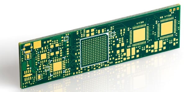
Where Hard Gold Plating Actually Gets Used
Hard gold shows up wherever a board gets touched, plugged, or pressed against something else on a repeat basis. The applications below share one trait: mechanical wear that a soft finish would not survive.
Edge connectors and gold fingers: Memory modules, graphics cards, and daughterboards that get inserted and removed repeatedly rely on hard gold fingers to keep contact resistance stable over thousands of cycles.
Keypad and membrane switch contacts: Industrial control panels and POS terminals press the same contact point tens of thousands of times over a product's life, and hard gold resists that wear better than any other plated finish.
Test points and bed-of-nails fixtures: Boards that get probed repeatedly during functional test benefit from hard gold's scratch resistance, since a worn test pad eventually causes false failures.
Automotive dashboard and infotainment connectors: Vibration and repeated connector cycling in a vehicle cabin push designers toward hard gold on gold finger interfaces for instrument clusters and head units.
Switch and relay contacts: Any mechanical switching contact that mates and unmates under load benefits from hard gold's stable contact resistance across its service life.
Once you know which parts of the board actually need that wear resistance, the next question is how hard gold stacks up against the alternatives on cost and performance.
Hard Gold vs. ENIG vs. Soft Gold: A Side-by-Side Comparison
The three gold finishes used on PCBs, hard gold, ENIG, and soft gold, trade off differently on hardness, thickness, and cost, and picking the wrong one for the job either wastes money or fails early.
The table below lines up the three finishes on the factors that actually drive a selection decision.
| Attribute | Hard Gold | ENIG | Soft Gold (Bonding) |
|---|---|---|---|
| Composition | Gold + 0.1-1% cobalt or nickel | Immersion gold over electroless nickel | Approximately 99.9% pure gold |
| Hardness (Knoop) | 120-300 | 60-85 | 60-85 |
| Typical gold thickness | 0.75-2.5 micrometers | 0.05-0.1 micrometers | 0.1-0.3 micrometers |
| Insertion cycle life | 1,000-10,000+ | Not rated for mechanical contact | A few hundred cycles |
| Solderability | Poor above about 17.8 microinches | Excellent | Good for wire bonding, not general soldering |
| Best fit | Edge connectors, switch contacts | BGA pads, fine-pitch SMT | Wire bond pads, RF/high-frequency pads |
Once the finish is chosen, the design decisions that follow determine whether the plating actually performs the way the spec sheet promises.
What Actually Drives a Clean Hard Gold Finger Design
Most hard gold plating problems trace back to layout decisions made before the board ever reaches the plating line, not the plating process itself.
Bevel angle: Gold fingers are typically beveled between 30 and 45 degrees so they slide smoothly into a connector slot without catching the plated edge.
Clearance from the board edge: Keep solder mask, silkscreen, and plated through holes clear of the gold finger area, generally with at least 1.0 mm of separation, so the plating boundary stays sharp.
Selective vs. full-body plating: Most designs only need hard gold on the fingers themselves, with the rest of the board finished in ENIG or another lower-cost option, which keeps material cost down.
Minimum board thickness: A board carrying gold fingers generally needs to be at least 1.0 mm thick so the fingers hold up mechanically during repeated insertion.
Conductor trace connecting the fingers: Fingers need to be tied together with a thin trace, commonly around 0.008 inch, so current reaches every finger evenly during plating; that trace is removed afterward.
These are exactly the kind of rules a fabricator's engineering team should be checking against your Gerber files before the job goes to plating, not after.
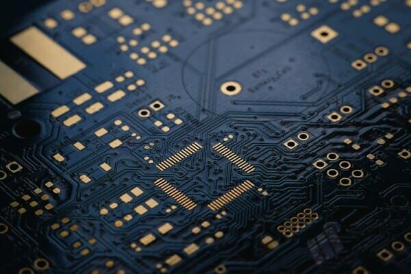
How PCBgogo Handles Gold Finger and Hard Gold Plating Checks
Since gold finger layout errors are easy to introduce and expensive to catch late, PCBgogo runs every hard gold order through a per-order design review before plating starts.
Both ENIG and electroplated hard gold on the same panel: PCBgogo supports dual-section and selective plating, so a board can carry hard gold fingers on one section and ENIG or another finish elsewhere without a second production run.
Bevel angle confirmed at intake: PCBgogo's current gold finger design rules support 30-degree beveling, and a Gerber file requesting a different bevel gets flagged during DFM review rather than plated as submitted.
AOI and X-ray inspection on every plated panel: Plating thickness and adhesion get checked after plating, not just at final QC, which catches masking or clearance errors before boards ship.
In-house fabrication start to finish: Because plating happens inside PCBgogo's own factory rather than through a subcontractor, adjustments identified during DFM review do not add a second vendor's lead time.
For gold finger designs specifically, it's worth checking your layout against PCBgogo's gold finger design guidelines before you submit files for quoting.
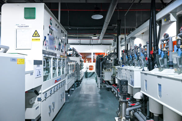
What to Verify Before Choosing a Manufacturer in China
Hard gold plating is unforgiving of shortcuts, so the questions below matter more here than they would for a standard ENIG order.
Certifications on file, not just claimed: Ask for the actual ISO 9001 and IATF 16949 certificates rather than a logo on the website, especially for automotive or industrial programs that require IATF compliance to pass their own audits.
A real DFM review before production: A supplier that checks your Gerber files for gold finger clearance, bevel angle, and trace connections before plating catches problems that are expensive to fix once the panel is already gold.
Plating thickness verification, not just a spec sheet: Ask what inspection method confirms actual deposited thickness, since X-ray fluorescence is the standard method, rather than trusting a nominal number in the quote.
RoHS documentation for every lot: RoHS compliance can vary between production runs if a supplier is not consistent about material sourcing, so ask for lot-specific documentation rather than a blanket certificate.
Turnaround time that matches your schedule: Selective hard gold plating adds process steps compared with standard ENIG, so confirm whether expedited options apply to hard gold orders specifically, since some suppliers quote fast turnaround only for standard finishes.
Working through that list before you place an order saves more time than any amount of back-and-forth after the boards arrive.
Frequently Asked Questions
What is the difference between hard gold and ENIG on a PCB?
Hard gold is an electrolytic gold alloy plated over nickel, built for mechanical wear resistance on contacts and connectors. ENIG is a thinner immersion gold layer over electroless nickel, built for solderability and flat pads rather than repeated mechanical contact.
How many insertion cycles can a hard gold connector survive?
Depending on plating thickness and contact force, hard gold edge connectors typically handle between 1,000 and 10,000 insertion cycles. Thicker deposits used in high-wear industrial or military connectors can exceed that range.
Can hard gold plated areas be soldered?
Hard gold can be soldered, but thicknesses above roughly 17.8 microinches risk gold embrittlement in the joint. Most designs keep hard gold off solderable pads entirely and apply it only to the finger or contact area.
Does hard gold plating cost significantly more than ENIG?
Yes, hard gold typically runs 15 to 30 percent more than ENIG on a finished board because of the extra masking, electrolytic setup, and gold volume involved. Selective plating, limited to just the fingers or contact points, keeps that premium manageable.
What board thickness is needed for gold fingers?
Most manufacturers require a minimum board thickness of around 1.0 mm for gold finger designs, since thinner boards do not hold up mechanically to repeated insertion. Check this against your specific fabricator's design rules before finalizing layout.
Is hard gold PCB plating RoHS compliant?
Yes, hard gold plating uses lead-free chemistry and the metals involved (gold, cobalt, nickel) are not restricted substances under RoHS. Ask your supplier for lot-specific RoHS documentation rather than relying on a general compliance statement.
Conclusion
Hard gold earns its higher cost on boards that get plugged in, pressed, or probed thousands of times, but it is the wrong choice for anything else. Getting the layout details right up front, and choosing a manufacturer that actually checks those details before plating, is what determines whether the finish performs the way it should.
When you're ready to move forward, PCBgogo's online quoting tool will price a hard gold or ENIG board once your Gerber files are uploaded.





