



 日本語
日本語
 한국어
한국어

Gold Finger PCB Manufacturing: Process and Design Guide
QUICK ANSWER Gold finger PCB manufacturing creates wear-resistant edge contacts by plating copper pads with nickel and specified gold, then profiling the card edge. A reliable drawing defines geometry, finish thickness, bevel, performance class, inspection, and mating conditions.
A gold contact row joins PCB fabrication, electroplating, and connector mechanics. This guide explains the process, design controls, inspection, repair, and fabrication data.
What Is a Gold Finger PCB?
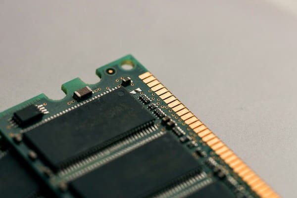
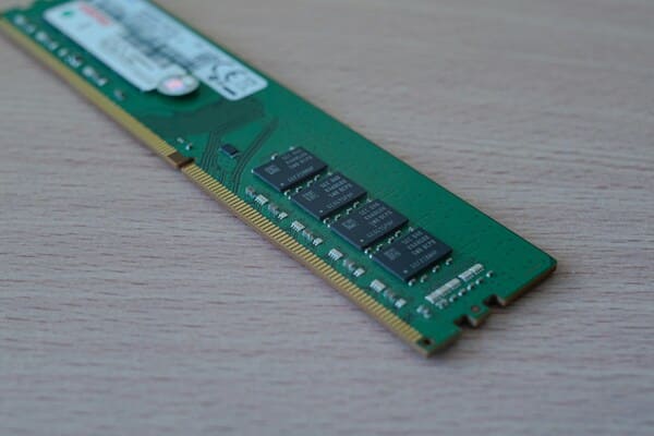
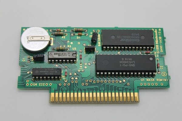
A gold finger PCB has plated contact lands along an edge that mates directly with a card edge connector. Examples include memory modules, graphics cards, industrial controllers, and test fixtures.
The contact begins as copper. Nickel provides a diffusion barrier and durable foundation, then gold supplies a corrosion-resistant contact surface. Repeatedly mated contacts normally use hard gold rather than immersion gold.
Gold fingers are the PCB contacts, while the connector is the mating socket. Their pitch, thickness, insertion depth, bevel, and wipe length must work as one system.
How Does the PCB Gold Finger Plating Process Work?
The PCB gold finger plating process prepares the copper contacts, deposits nickel and hard gold, and finishes the card edge without damaging the contact area. The exact sequence varies by factory and panel design, but it includes seven functional stages.
Panel engineering: CAM engineers verify geometry, clearance, bevel, and the temporary electrical path. Every finger must connect to a plating bus, rail, or removable tab.
Copper preparation: The contacts are formed with the outer layer, then cleaned and activated.
Selective masking: Noncontact areas are protected to control gold use and separate connector contacts from solderable pads.
Nickel deposition: Nickel is electroplated over exposed copper to limit copper migration and support the gold layer.
Hard gold deposition: An external current deposits controlled gold alloy. Cobalt or nickel may be added to improve wear resistance.
Profiling and beveling: Temporary connections are removed, the board is routed, and the edge is beveled where required.
Inspection: The fabricator verifies appearance, adhesion, dimensions, thickness, and continuity.
The current MIL DTL 45204 covers electrodeposited gold on metallic surfaces and calls for an antidiffusion underplate such as nickel over copper-rich surfaces. It is a procurement specification for specified applications, not an automatic requirement for every commercial PCB.
Should Gold Fingers Use Hard Gold or ENIG?
Hard electroplated gold is normally the stronger choice for repeatedly mated edge contacts, while ENIG is better suited to flat solderable pads and low wear surfaces. Selection depends on mating cycles, contact force, environment, cost, and the product drawing.
| Finish | Deposition method | Wear resistance | Best fit |
|---|---|---|---|
| Hard gold over nickel | Electrolytic, selective | High | Repeatedly mated card edge contacts |
| ENIG | Electroless nickel plus immersion gold | Lower under sliding wear | Component pads and low cycle contacts |
Do not copy gold thickness from a generic table. Specify it from connector duty, the governing standard, the reliability plan, and fabricator review.
Which Design Decisions Control Gold Finger Reliability?
Gold finger reliability is controlled by mating geometry, plating access, contact sequencing, copper clearance, and clear fabrication notes.
Mating geometry: Match card thickness, pitch, insertion depth, and bevel to the connector data sheet.
Plating access: Provide a temporary electrical path to every contact. Isolated fingers can require special panel engineering or removable tabs.
Contact sequencing: Use staggered pad lengths only for deliberate first mate or last break behavior. A longer ground contact can engage before shorter signal contacts.
Copper near the bevel: Keep internal copper and plated features away from the edge. Clearance depends on stackup, thickness, bevel, and factory capability.
Contact surface clearance: Keep solder mask and legend ink outside the wipe area. Raised coating or residue can interfere with spring contact.
Edge profile: Define bevel angle, remaining thickness, and where the bevel starts and stops.
A 1.0 mm clearance or 45-degree bevel may suit one process and fail another connector. Put functional requirements on the drawing, then obtain a DFM review from the selected fabricator.
How Should Gold Finger PCBs Be Inspected?
Gold finger PCB inspection should verify contact, wear, and insertion controls rather than color alone. A bright surface can still have thin plating, contamination, burrs, or incorrect geometry.
IPC 6012F: This is the current performance specification for rigid printed boards. IPC released Revision F in 2023. State the applicable class and add requirements in procurement documents.
IPC A 600: This visual acceptance standard covers edge contact plating, burrs, and overplate adhesion. IPC identifies IPC A 600 as its workmanship acceptance reference.
Product drawing: The drawing defines contact dimensions, finish, thickness, bevel, and mating requirements. IPC classification alone does not select these values.
Inspection plan: Thickness measurement, dimensional checks, electrical testing, adhesion evaluation, and cleanliness controls should match the failure risks.
Protect the inspected surface from fingerprints, abrasion, loose packaging, and cleaning residues after plating.
When Is PCB Gold Finger Repair Acceptable?
PCB gold finger repair is acceptable only when an approved procedure can restore geometry, adhesion, conductivity, and wear life. Cleaning contamination is different from rebuilding a damaged contact.
Identify the defect: Separate contamination from scratches, exposed base metal, lifted plating, delamination, or a cracked trace.
Check the service class: A test adapter and safety-critical board carry different repair risks.
Use an approved procedure: Define materials, workmanship, inspection, and acceptance. Do not improvise with solder, abrasives, or conductive paint in the wipe zone.
Confirm geometry: A raised repair can damage the socket or concentrate wear.
Retest the interface: Inspect the surface and verify continuity and product-specific functions before release.
IPC 7711/21D is the current IPC repair document. The product authority must still approve a repaired contact. If wear reaches copper, the pad lifts, or reliability is critical, replacement or professional replating is often safer.
What Should Be Sent to the PCB Manufacturer?
A complete gold finger PCB manufacturing package defines both board geometry and expected contact performance. Gerber or ODB++ data can show copper shape but may not communicate finish, bevel, or reliability requirements.
Contact definition: Identify each finger, board side, pad length, pitch, and staggered sequence.
Finish callout: State the finish, nickel and gold requirements, and selectively plated area.
Mechanical controls: Give final board thickness, connector edge dimensions, bevel angle, remaining thickness, and tolerances.
Acceptance requirements: State performance class, visual criteria, tests, sampling, and reports.
Mating information: Supply the connector part number, expected cycles, environment, and sequence.
A note saying only "gold fingers required" is not enough. Resolve missing thickness, bevel, inspection, and connector data before fabrication.
How PCBgogo Supports Gold Finger PCB Manufacturing
Gold finger production is easier to source when the fabricator publishes finish and edge processing limits.
Connector finishes: PCBgogo lists hard gold, ENIG, and selective gold fingers among its manufacturing options.
Edge processing: Its current FR4 table lists gold finger bevel angles from 30 to 45 degrees, a bevel depth of at least 1 mm, and a minimum board thickness of 1.2 mm for that process.
Capability review: These are factory limits, not universal rules. Send exceptions for engineering review.
Review the current PCBgogo FR4 PCB manufacturing capabilities before requesting a quote.
Frequently Asked Questions About Gold Finger PCBs
Why is nickel placed under the gold on PCB fingers?
Nickel forms a barrier between copper and gold while providing a harder supporting layer. It reduces copper diffusion and helps the contact retain its intended surface properties.
Can ENIG be used for PCB gold fingers?
ENIG can suit low wear or low cycle contacts if product requirements allow it, but it resists repeated sliding wear less effectively than hard gold. Confirm the choice with the connector supplier and fabricator.
Does every gold finger PCB need a beveled edge?
No. A bevel is needed only when connector geometry and insertion require it. Use the connector specification to define angle and remaining edge thickness.
Can worn gold fingers be repaired with solder?
Solder is not a routine repair for the connector wipe area because it changes hardness, thickness, and geometry. Use an approved process or replace the board when wear or base metal exposure threatens reliability.
What causes uneven gold plating?
Uneven plating can result from surface preparation, current distribution, masking, bath control, plating bus contact, or panel geometry. Thickness measurement is necessary because color cannot confirm uniformity.
Conclusion
Reliable gold finger PCB manufacturing starts with the mating connector and a drawing that controls finish, thickness, contact sequence, bevel, inspection, and repair authority. Resolve those requirements during DFM review so the finished contact is manufacturable, measurable, and suited to its real insertion duty.





