




 日本語
日本語
 한국어
한국어

Foldable PCB Manufacturing: PCBgogo provide high Quality Solutions
KEY DEFINITION A practical design and sourcing guide for reliable flex and rigid-flex products. A foldable PCB is a practical circuit solution for products that must wrap, hinge, or fit around a small three-dimensional enclosure. The right answer is usually a dynamic flex circuit, a static flex interconnect, or a rigid-flex assembly, chosen based on the required bend life, component support, and installed shape. Production success depends on treating the bend area as a mechanical feature, not simply a thin PCB.
A foldable electronic product often fails at the point where electrical routing meets mechanics. A cable can consume space, add connectors, and complicate assembly; a conventional rigid board cannot pass through a hinge or follow a curved housing. Foldable PCB manufacturing solves this packaging problem by integrating conductors on a flexible dielectric, with rigid islands where components need support.
This guide explains how to select a foldable PCB type, design the bend zone, prepare fabrication data, and judge the total cost. It focuses on decisions a hardware team can use before releasing a prototype or production RFQ.
Foldable PCB Types
Foldable PCB types differ mainly in whether the flex section moves repeatedly and whether component areas must be structurally rigid. Selecting the structure early prevents expensive stackup changes after enclosure tooling has begun.
The comparison below separates the three common options. "Foldable" should not imply unlimited folding: every design needs a defined bend radius, bend direction, and installation geometry.
| Type | Best fit | Key design implication | Relative cost |
|---|---|---|---|
| Static flex PCB | One-time fold during assembly, such as a display or sensor interconnect | Use a documented installation radius; avoid later rework bends | Medium |
| Dynamic flex PCB | Repeated hinge or motion cycles | Use rolled-annealed copper where possible and keep the bend zone free of vias and pads | Medium to high |
| Rigid flex PCB | Component-bearing rigid areas joined by flex tails | Define rigid-to-flex transitions, stackup, and panel handling together | High |
A simple flex tail is usually the most economical route when the fold is installed once. When the circuit must travel through a hinge every day, dynamic-flex rules govern copper, routing, and strain relief. Rigid flex becomes valuable when replacing separate boards, cables, and connectors improves assembly or reliability.
Foldable PCB Design
Foldable PCB design starts by drawing the actual folded state, including hinge axis, clearance, bend radius, and every location that becomes inaccessible after assembly. The layout team should receive the mechanical envelope before trace routing, not after it.
Keep the bend zone clean: Do not place vias, solder joints, component pads, abrupt trace-width changes, or sharp copper corners in the active bend area. These features concentrate strain and can start a crack.
Route with the bend: For a simple bend, run traces perpendicular to the bend line so each conductor shares the strain over its width. Use smoothly curved traces where routing changes direction, rather than right-angle geometry.
Set radius from the finished stack: A practical static-flex starting point is a bend radius of at least 10 times the finished flex thickness. Repeated-motion designs need a larger radius and a review based on copper type, layer count, and target cycle life.
Balance the flex stack: Keep copper and dielectric construction as symmetrical as the function allows. An unbalanced build can curl after lamination, making assembly fixtures and adhesive placement harder to control.
Add support only where needed: FR-4, polyimide, metal, or other stiffeners can reinforce connector and component areas, but the stiffener edge must stop clear of the bend. Specify its thickness, adhesive, and location in the drawing.
These rules lead directly to manufacturing choices. A design that looks routable in CAD can still be difficult to laminate, drill, panelize, or inspect if the documentation does not identify its flex zones.
Foldable PCB Manufacturing Requirements
Foldable PCB manufacturing requires the fabricator to control material flow, copper patterning, coverlay registration, and handling without damaging thin flexible sections. The release package should make the intended mechanical behavior unambiguous.
Material callout: Specify polyimide or PET where appropriate, adhesive or adhesiveless construction, copper type, finished copper by layer, coverlay, and any shielding film. Polyimide is commonly selected for higher-temperature processing and demanding flex use.
Fabrication drawing: Mark static and dynamic bend zones, bend lines, minimum installed radius, bend direction, stiffener outline, and areas that must remain flat. Include a folded assembly view when the circuit fits a tight enclosure.
Stackup and impedance: Provide the approved stackup and impedance targets for signal-critical lines. A flex stack cannot be assumed to behave electrically like an FR-4 stack of similar thickness.
Panel and assembly plan: Thin flex needs carrier rails or a fixture for SMT processing. Define fiducials, tooling holes, breakaway method, and whether the board is assembled before or after folding.
Inspection plan: Specify electrical test and the acceptance criteria for exposed copper, coverlay opening alignment, surface finish, and dimensional features. If reliability is cycle-dependent, agree on the bend test method before production.
A manufacturing review is most useful before the mechanical design is frozen. It can expose coverlay, stiffener, and panel constraints while the enclosure still has room for adjustment.
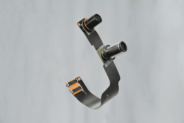
Advantages and Limitations of Foldable PCB
A foldable PCB trades higher fabrication complexity for better packaging and fewer interconnects. The decision should be based on total product cost and reliability, not bare-board price alone.
| Advantages | Limitations to manage |
|---|---|
| Fits hinges, curves, and compact three-dimensional housings | Needs bend-radius control and accurate mechanical documentation |
| Can replace wire harnesses and board-to-board connectors | Material, coverlay, stiffener, and lamination steps raise unit cost |
| Reduces connection points that can loosen under vibration | Repair after installation is usually harder than for cable assemblies |
| Supports lighter assemblies and repeatable folded geometry | Dynamic use requires conservative design and validation testing |
The strongest business case appears when a flex circuit removes several manual cable connections, reduces enclosure volume, or prevents a recurring connector failure. If the product has ample space and no moving interface, a standard rigid PCB and cable may still be the better solution.
Foldable PCB Cost and Why It Is Higher
Foldable PCB cost is higher than a comparable rigid PCB because its material set, process controls, and production yield are more sensitive. The cost increase is not caused by flexibility alone; it comes from the manufacturing features needed to preserve it.
Polyimide films, coverlay, specialized adhesives, rolled copper, stiffeners, and shielding films add material cost. Fine flexible panels also need careful handling, dedicated tooling, and often support rails through assembly. Multilayer flex and rigid flex add registration, lamination, drilling, plating, and layer-transition complexity, so scrap risk carries more weight in the quote.
To control cost without weakening the product, keep active bend zones single-layer when feasible, avoid unnecessary rigid-flex layers, standardize finishes, and use stiffeners only under connectors or components. Release a complete drawing with one agreed stackup; late changes to thickness or stiffener placement can require a new manufacturing approach.
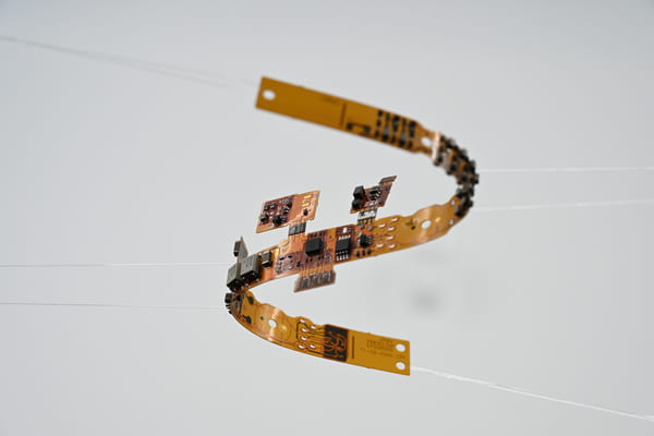
Current Applications for Foldable PCB
Foldable PCB is especially useful in current products where miniaturization, motion, and dense sensing must coexist. The following applications use flex for a concrete packaging or reliability purpose, not merely because it is thin.
Foldable smartphones and dual-screen devices: Flex circuits carry signals through the hinge and connect cameras, antennas, displays, and sub-boards in a limited interior volume.
AR and VR headsets: Flexible interconnects route between display modules, tracking cameras, proximity sensors, and compact main boards while following a curved wearable frame.
Wearable health devices: Smart rings, patches, and continuous-monitoring wearables use flex to conform around the body and join sensor modules to batteries or charging contacts.
Robotics and autonomous drones: Articulated joints, gimbals, and compact sensor pods benefit from low-mass flex routing that avoids bulky cable loops and reduces motion interference.
Electric vehicle battery and cockpit electronics: Flexible circuits can package distributed sensing, display, and lighting connections in constrained assemblies, provided temperature, vibration, and service requirements are designed in.
Portable medical and diagnostic instruments: Handheld ultrasound accessories, wearable therapy devices, and compact imaging modules use flex where low weight, repeatable assembly, and controlled signal routing matter.
Across these applications, the common lesson is mechanical integration. The circuit must be designed alongside the enclosure, hinge, fixture, and service path.
PCBgogo as a Foldable PCB Manufacturing Partner
PCBgogo is a practical choice for foldable PCB projects when the sourcing team needs one manufacturer to review the flexible construction and support the path from prototype to assembly. The value is in aligning the manufacturing package with the behavior of the flex area before a production order is released.
Relevant flexible options: PCBgogo supports flexible PCB material choices including PI and PET, coverlay-related construction, stiffeners, shielding options, and common surface finishes. These are the features that turn a routed flex circuit into an installable assembly.
Capability review for complex builds: For designs that combine rigid and flex areas, the team can assess stackup, layer transition, fine routing, laser-hole needs, and impedance requirements against the supplied drawing rather than relying on generic flex rules.
Manufacturing and assembly continuity: A single workflow for PCB fabrication, component sourcing, assembly, inspection, and testing can reduce handoffs for projects that need rails, fixtures, or controlled folding during assembly.
Clear RFQ inputs: Providing bend requirements, finished thickness, copper weights, coverlay openings, stiffener details, and expected quantity enables a more useful engineering response and reduces avoidable revisions.
The best next step is to submit the mechanical constraints with the Gerbers, drill data, stackup, and fabrication drawing. That gives PCBgogo enough information to identify manufacturability questions before the flex design reaches the production floor.
PCBgogo - Reliable, High-Quality PCB Manufacturing
Save time and money with an all-in-one solution for PCB fabrication, assembly, and parts. Reduce vendor coordination, avoid split shipments, and get consistent, reliable quality.
Get Free Quote >
Summary
Foldable PCB manufacturing delivers its greatest value when it replaces an unreliable cable path or enables a compact product shape that a rigid board cannot reach. Choose static flex, dynamic flex, or rigid flex from the real motion and support requirements, then protect the bend zone through layout, stackup, and clear manufacturing documentation. A complete early review is usually less expensive than correcting a flex failure after tooling and assembly are in motion.
Frequently Asked Questions
What is the difference between a foldable PCB and a flexible PCB?
A foldable PCB is a flexible or rigid-flex circuit designed to be bent or folded into a defined installed shape. A flexible PCB is the broader material category, and it may be used flat, statically folded once, or dynamically flexed many times.
Can a foldable PCB be folded repeatedly?
Yes, but only if it is designed as a dynamic flex circuit. Repeated folding requires a controlled bend radius, suitable copper construction, no vulnerable features in the bend zone, and validation against the intended motion cycle.
What files should I send for a foldable PCB quote?
Send Gerber or ODB++ fabrication files, drill data, a layer stackup, a fabrication drawing, and a folded mechanical view. The drawing should identify bend zones, bend direction, radius, stiffeners, coverlay, and any impedance requirements.
Why are stiffeners used on a foldable PCB?
Stiffeners reinforce connector and component areas so they can withstand insertion, soldering, and handling. They should not extend into the active bend zone, where they would create a stress concentration.
Is rigid flex always better than a cable and rigid boards?
No. Rigid flex is justified when it saves space, removes failure-prone interconnects, or simplifies a complex assembly. A rigid PCB plus cable can be more economical when the product has space, limited vibration, and no tightly controlled folded geometry.





