
 日本語
日本語
 한국어
한국어

Edge Computing PCB: Design, Application & Hardware Overview
The shift toward distributed intelligence is reshaping how industries design electronics. At the center of this transformation is the edge computing PCB — the physical hardware layer that makes real-time, low-latency processing possible without relying on distant cloud servers. Whether it powers an autonomous vehicle navigating a busy intersection, a robotic arm on a factory floor, or an IoT sensor cluster in a smart city, the PCB inside every edge AI computer must meet a uniquely demanding set of requirements.
This guide covers everything engineers and procurement teams need to know about edge computing PCBs: what makes their design different, which applications are driving demand, and how to choose the right manufacturing approach.
What Is an Edge Computing PCB?
An edge computing board is a printed circuit board engineered to run compute-intensive workloads — AI inference, sensor fusion, real-time control — at or near the point of data generation, rather than sending raw data to a centralized cloud. Unlike typical server boards housed in climate-controlled data centers, edge computing PCBs must often operate in harsh, space-constrained, and thermally challenging environments.
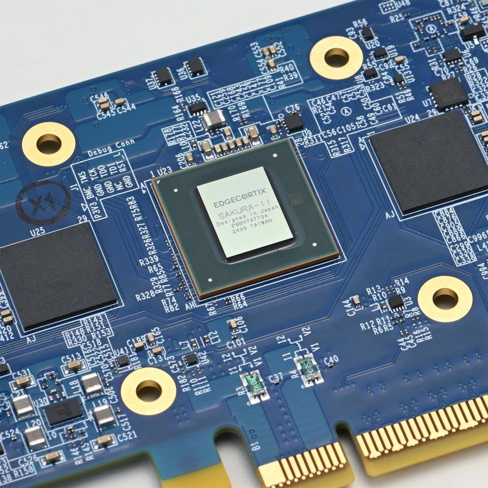
The global edge computing market is projected to exceed $200 billion by 2030, driven by the explosion of IoT endpoints, autonomous systems, and latency-sensitive AI applications. This growth puts enormous pressure on PCB designers to deliver boards that combine high performance with rugged reliability — often in form factors far smaller than traditional compute platforms.
Why Edge Computing PCB Design Is Different
Standard server PCBs are optimized for throughput and thermal headroom, with large footprints and active cooling infrastructure. Edge computing PCBs face a very different set of constraints:
Compact Form Factor Edge nodes must fit into vehicle cabins, industrial enclosures, and outdoor equipment housings. High-density interconnect (HDI) technology is almost always required to pack powerful SoCs, AI accelerators, memory, and connectivity into minimal board area.
Thermal Management Without Active Cooling Many edge deployments cannot rely on fans or liquid cooling. PCB designers must use thermally conductive substrates, copper pours, embedded thermal vias, and carefully planned component placement to manage junction temperatures passively.
Signal Integrity at Speed Modern edge AI computers process sensor data streams exceeding 25 Gbps. Maintaining signal integrity at those speeds requires precise impedance control, advanced stackup design, low-loss dielectric materials, and careful routing of high-speed differential pairs.
Environmental Robustness Industrial edge computing deployments routinely expose PCBs to vibration, temperature swings from –40°C to +85°C, humidity, dust, and EMI. Material selection and surface finish choices directly determine long-term reliability.
Power Efficiency Battery-powered or energy-harvested edge nodes have strict power budgets. The PCB must support efficient power delivery networks, dynamic voltage scaling, and low-leakage component choices.
Key Design Considerations for Edge Computing PCBs
HDI Technology and Miniaturization
High-density interconnect PCBs use micro-vias (as small as 0.05 mm), staggered or stacked blind and buried vias, and sequential lamination to achieve routing density impossible with conventional through-hole technology. For an edge AI computer integrating a high-end SoC, LPDDR5 memory, PCIe, and multiple sensor interfaces, HDI is typically the only viable path.
Material Selection
The substrate material governs thermal, electrical, and mechanical performance across the board's service life:
· Standard FR4 (e.g., Isola 370HR, IT-180A) — suitable for non-critical signal layers in moderate environments
· High-frequency laminates (Rogers RO4000 series, Taconic RF-30) — essential for RF front-ends and high-speed serial links in edge AI hardware
· High-speed laminates (Panasonic MEGTRON-6, Isola I-Tera MT40) — low-loss dielectrics that preserve signal integrity at PCIe Gen4/5 and 25G+ Ethernet speeds
· Thermally conductive substrates — reduce junction temperatures by up to 30% in passively cooled enclosures
· Halogen-free materials — required for RoHS compliance and increasingly specified in automotive and industrial edge computing programs
Impedance Control and Stackup Design
High-speed signals demand tight impedance tolerances, typically ±10% or better. A well-designed stackup for an edge computing board separates power planes, reference planes, and signal routing layers to minimize crosstalk and return path discontinuities. Differential pair routing, length matching, and via stub management are all critical for signals above 10 Gbps.
Power Delivery Network (PDN)
Edge boards often supply multiple voltage rails to SoCs, FPGAs, memory, and RF components simultaneously. The PDN must be modeled for impedance across the frequency range of interest, with decoupling capacitors placed as close as possible to power pins. Heavy copper layers (2–4 oz) are sometimes used in high-current sections.
Conformal Coating and Protection
For outdoor, automotive, and industrial edge computing deployments, conformal coating is applied after assembly to protect against moisture, chemicals, and contamination. Potting compounds offer even higher protection for the most demanding environments.
Edge Computing PCB Applications in Autonomous Vehicles and Industrial Systems
Edge computing PCBs are designed to support real-time decision-making in environments where cloud processing is too slow or unreliable. The most common applications are in autonomous vehicles and industrial systems, where latency, reliability, and on-device intelligence are critical.
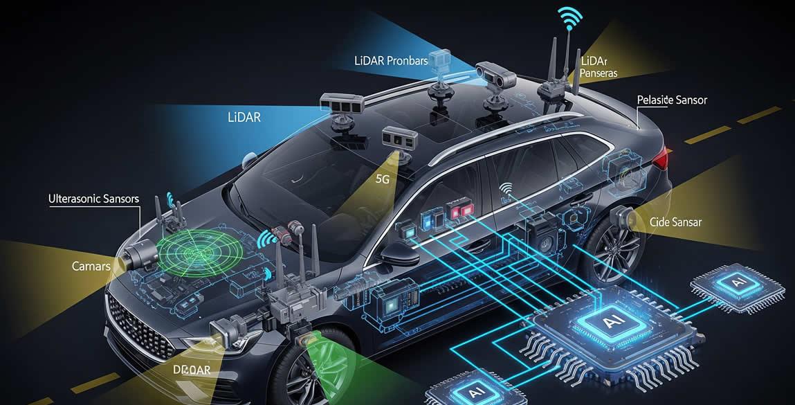
In autonomous vehicles, edge computing enables the processing of large-scale sensor data directly inside the vehicle. Key functions include:
· Sensor fusion, combining data from lidar, radar, cameras, and other sensors into a real-time driving model
· ADAS features such as lane keeping, adaptive cruise control, and emergency braking with millisecond-level response
· V2X communication for interaction with traffic infrastructure and nearby vehicles via 5G or DSRC
· HD mapping and localization (SLAM) for accurate positioning and path planning
To support these workloads, automotive-grade PCBs must meet strict requirements such as AEC-Q qualification, wide temperature tolerance (–40°C to +125°C), strong EMI shielding, and long-term reliability under vibration and harsh road conditions.
In industrial environments, edge computing PCBs power real-time control and AI-driven automation under continuous operation. Typical applications include:
· Machine vision for defect detection and quality inspection on production lines
· Predictive maintenance using sensor data to detect equipment failures early
· Real-time process control with closed-loop feedback systems
· Robotics and cobot control for motion planning and safety monitoring
Compared to automotive use, industrial PCBs focus more on EMI resistance, thermal management, and long lifecycle stability, often requiring IPC Class 3 manufacturing standards and reinforced mechanical design for high-vibration environments.
Edge AI Computer Hardware: What's Inside the PCB
A fully featured edge AI computer PCB typically integrates:
| Function | Hardware | PCB Implication |
|---|---|---|
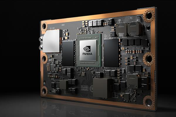
| AI inference | GPU / NPU / custom AI accelerator (e.g., NVIDIA Jetson, Hailo, Qualcomm AI) | High-power PDN design, advanced thermal management, dense BGA routing |
| General compute | Multi-core ARM or x86 SoC | High-speed DDR5 / LPDDR5 signal routing with strict timing control |
| Memory | LPDDR5 or DDR5 (6400+ MT/s) | Strict length matching, impedance control, low skew routing |
| Storage | PCIe NVMe SSD / eMMC | PCIe Gen3/Gen4 differential pair routing, signal integrity optimization |
| Connectivity | 5G/LTE modem, Wi-Fi 6E, Gigabit Ethernet | RF PCB design, impedance-controlled antenna routing, EMI shielding |
| Sensor interfaces | MIPI CSI-2, USB 3.2, CAN FD, LIN | Mixed-signal isolation, high-speed differential routing |
| Power management | Multi-rail PMIC | Power distribution network (PDN) design, optimized decoupling capacitor placement |
The integration density of modern edge AI hardware means many of these functions coexist on a single compact board, making HDI PCB technology and advanced stackup design essential rather than optional.
Cost Optimization Strategies for Edge Computing PCBs
High performance doesn't have to mean uncontrolled cost. Proven strategies include:
Optimize Layer Count Every additional layer adds manufacturing cost. Working with your PCB manufacturer early to assess whether layers can be consolidated — through better routing, via-in-pad technology, or design simplification — can reduce costs significantly without sacrificing performance.
Match Materials to Performance Needs Not every layer requires a low-loss high-frequency laminate. A hybrid stackup, using advanced materials only where signal integrity demands it and standard FR4 elsewhere, cuts material costs while maintaining performance.
Apply Design for Manufacturing (DFM) from Day One DFM review catches problems before they reach the fab: insufficient via-to-trace clearances, unmanufacturable pad sizes for fine-pitch BGAs, thermal relief configurations that impede soldering. Fixing these in design is orders of magnitude cheaper than fixing them in production.
Streamline Testing to Critical Parameters Edge computing PCBs require thorough testing, but over-testing wastes budget. Focus automated optical inspection (AOI), X-ray inspection, and functional testing on the signal integrity, power delivery, and thermal performance parameters that actually determine field reliability.
Manage Component Sourcing Proactively Supply chain disruptions have taught the industry that single-source components are a liability. Design-in alternate component footprints where possible, and work with your manufacturer to maintain safety stock on long-lead-time items like AI SoCs and high-speed memory.
Choosing the Right Edge Computing PCB Manufacturer
Not all PCB manufacturers can support the design complexity of edge computing boards. Key capabilities to evaluate:
· HDI fabrication capability — micro-via formation (laser drill), sequential lamination, via-in-pad plating
· High-frequency and high-speed laminate experience — proven processes with Rogers, Isola, Panasonic MEGTRON, and similar materials
· Impedance control accuracy — ±5% or better with coupons and TDR verification
· Automotive and industrial certifications — IATF 16949, IPC-6012 Class 3, RoHS, ISO 9001
· Full-stack services — PCB fabrication, component sourcing, assembly, functional testing, and conformal coating under one roof reduces handoff risk and accelerates time to market
As a reliable full-stack PCB manufacturing service provider, PCBgogo owns all the above core capabilities, specializing in high-precision edge computing PCB customization and mass production. You can visit PCBgogo's official homepage to learn more professional solutions and submit inquiries for customized quotes.
Future Trends in Edge Computing PCB Technology
Embedded computing — embedding active dies and passive components directly into PCB substrates reduces parasitics and improves density beyond what surface-mount assembly achieves.
AI-optimized silicon proliferation — purpose-built NPUs and AI accelerators with ever-higher TOPS/watt ratios are arriving at the edge, demanding PCB platforms that can handle their thermal and power delivery requirements.
Edge-cloud collaboration architectures — next-generation edge deployments are not monolithic but tiered, with in-vehicle processing collaborating with roadside MEC servers and cloud infrastructure. PCB platforms at each tier have different compute, connectivity, and form-factor requirements.
5G integration — as 5G NR becomes the connectivity fabric for V2X and industrial IoT, edge AI computers increasingly integrate 5G modems, requiring careful co-design of the RF and baseband PCB sections to manage interference and antenna placement.
Sustainability and halogen-free design — environmental regulations and customer sustainability commitments are driving broader adoption of halogen-free, RoHS-compliant materials throughout the edge computing PCB supply chain.
Summary
The edge computing PCB is the hardware foundation of the distributed intelligence era. From edge computing in autonomous vehicles to industrial edge computing on factory floors, from sensor fusion edge computers to IoT gateways, the demands placed on these boards — miniaturization, thermal management, signal integrity, environmental robustness — are unlike those of any previous generation of electronics.
Success in designing and manufacturing edge computing boards requires close collaboration between PCB designers, materials engineers, and manufacturing partners from the earliest stages of a program. The right combination of HDI technology, carefully matched materials, rigorous DFM, and end-to-end supply chain management delivers edge computing boards that perform reliably at the most demanding points in modern intelligent systems.





