




 日本語
日本語
 한국어
한국어

Edge AI Hardware PCB Design for Reliable Industrial Vision
Edge AI hardware places inference near the camera, sensor or machine, so its PCB must route a dense processor and memory, preserve clean high speed signals, and carry heat into a real cooling path. The example below specifies a 16 layer industrial vision board using blind and buried vias, copper filled microvias, controlled impedance, and a chassis heat spreader. Its dimensions and test limits are engineering targets, not reported customer results.

A 16 layer board for an industrial vision accelerator
Consider a fanless inspection camera installed above a packaging line. Two image sensors feed an accelerator that identifies missing labels and damaged seals locally, then sends only decisions and cropped evidence to the plant network. The module needs LPDDR memory, nonvolatile storage, a host interface, Ethernet, power conversion, and camera connectors within a 90 × 70 mm board outline. The design target is a 16 layer, 1.6 mm HDI PCB with an approximately 0.5 mm pitch accelerator BGA and a 15 W sustained compute budget. These are proposed design inputs; the exact chip, package, and power figure must come from the selected device data sheet.
Why 16 layers? The proposed stackup gives each major function room without sacrificing continuous reference planes:
Two outer layers handle component breakout around the accelerator and memory BGAs.
Four internal ground layers provide nearby references for critical signal routes.
Two power layers distribute the accelerator’s multiple rails, while the remaining signal layers separate memory, camera, and host traffic.
That separation helps keep memory close to the processor, limits unnecessary layer changes, and preserves copper for power and heat spreading. Routing, power integrity, and signal integrity checks must confirm this allocation before release.
Once those electrical and mechanical needs establish the stackup, PCBgogo can review how to build it. Its published HDI capability covers 16 layer small and medium volume boards and offers blind and buried vias with sequential lamination. The design team should submit the layer map, copper weights, dielectric choices, via spans, and impedance classes together, because meeting a layer count alone does not establish that the complete construction is manufacturable.
Blind and buried vias that free the BGA escape
A blind via connects an outer layer to one or more inner layers without crossing the whole board; a buried via connects only internal layers. For this board, a proposed 2+12+2 construction uses two sequential build up layers on each side of a 12 layer core. Laser drilled L1–L2 and L2–L3 microvias escape the accelerator and memory. Buried L3–L14 vias connect internal routing where required. Staggering the adjacent microvias avoids a tall stacked column unless the final fanout proves it necessary.
The 0.5 mm pitch BGA leaves little room for a conventional dog bone escape in its inner rows. A proposed 0.10 mm laser microvia beneath selected pads creates a short path to the next routing layer, while 3/3 mil lines are reserved for the tightest escape channels; less constrained traces stay wider. Copper filled microvias and planar via in pad recover pad area without leaving an open hole that can draw solder away during assembly. PCBgogo publishes 0.10 mm production microvias and the relevant fill and via in pad processes, so its engineering team can check the combined geometry against the actual package footprint and stackup.
This via plan has a measurable benefit: short transitions avoid the unused barrel associated with a full depth via, and selective drill spans leave more room for planes and routing. It does not guarantee a passing high speed channel. The designer must model the package, breakout, vias, traces, and connector as one path, then inspect the manufactured geometry and test the assembled link.
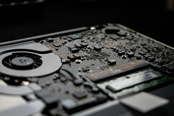
The proposed fabrication and validation targets
The table records a design brief, not achieved production data. In particular, a 100 Ω differential target is only valid for an interface whose data sheet calls for it. Trace width is calculated from the approved dielectric thickness, copper profile, and material properties. PCBgogo publishes standard HDI impedance tolerance of ±10%; a tighter target requires a qualified build and test agreement. Add TDR coupons on the same panel, and compare measured values with the released stackup.
| Item | Proposed value | Why it matters |
|---|---|---|
| Construction | 16 layers, 2+12+2, 1.6 mm | BGA escape plus continuous reference planes |
| Laser microvia | 0.10 mm nominal, staggered | Short outer layer transitions |
| Fine lines | 3/3 mil only near BGAs | Routing density with margin elsewhere |
| Signal channels | 100 Ω differential nominal, final geometry by field solver | Matched high speed host and camera links |
| Power copper | 1 oz internal power planes, subject to current analysis | Lower distribution resistance |
| Thermal path | Via arrays, inner copper, spreader and chassis contact | Moves heat beyond the board |
| Acceptance tests | Impedance coupon, microsection, electrical test, thermal run | Checks the actual fabricated and assembled board |
Signal integrity and power delivery on a crowded board
The signal strategy begins with the return path. Three layout checks matter most on this board:
Route each fast pair over a solid adjacent ground plane; avoid cutting that plane with power islands or via antipads.
At a layer change, place a nearby ground return via where the geometry permits.
Match pair timing to the selected interface budget, including skew from the package and connector as well as the PCB.
Back drilling is an available PCBgogo process for a through via that leaves an excessive stub, but use it only after channel analysis shows the stub matters.
Keep memory close to the accelerator and assign its own routing region. The BGA breakout may use microvias, but memory timing depends on the complete bus topology, reference planes, and termination scheme. Power delivery needs equal attention: put small decoupling capacitors near the accelerator power pins, use short via connections to planes, and analyze transient voltage drop for the chosen device. A 1 oz plane is a proposal, not evidence that the rail can carry any particular current. Widen copper and add parallel connections where current density or DC loss demands it.
A manufacturing review should compare the impedance table, cross section, drill map, and copper distribution together. Fine traces next to heavy power copper can require different etch allowances. A low loss dielectric is an option where channel loss warrants it; PCBgogo lists several qualified high speed materials. Choose the material from the actual signal rate, route length, and loss budget rather than selecting an expensive laminate by default.
A heat path designed for continuous inference
Heat leaves an accelerator through its package into the top side heat spreader and, where the package allows, through thermal pads and vias into board copper. For this proposed camera, specify a 15 W sustained workload at a 40°C enclosure ambient. Reserve a copper region beneath the power stage and a mechanically controlled interface from the accelerator heat spreader to the aluminum chassis. If exposed thermal pads are present, use filled and capped vias compatible with assembly so solder does not wick into open holes. An inner copper plane spreads some heat laterally; it is not a substitute for contact to the enclosure.
The qualification target is a two hour run in the final enclosure at the intended model and image rate. The proposed pass criteria are:
No accelerator thermal throttling during the sustained workload.
No camera or host interface error accumulation during the run.
All component temperatures remain below their data sheet limits at the specified ambient temperature.
Accelerator telemetry, regulator case temperature, chassis contact temperature, ambient temperature, and rail voltage are recorded throughout.
These are acceptance criteria, not a claim that a PCBgogo build has passed them. The report should also record the thermal interface material, clamp force, firmware version, and workload, because changing any one of them can change the result.
Copper filled microvias, larger internal copper areas, and a chassis spreader form the proposed thermal system. Their contribution should be checked by simulation before fabrication and by measurement after assembly. If the package dissipates most heat through its top surface, improving its heat sink contact will matter more than adding vias under unrelated pads. This is why the board and enclosure teams need one shared thermal drawing.
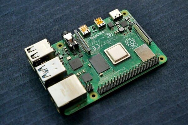
What success would look like in the camera
The camera is intended to inspect one package every 250 ms on a conveyor, while keeping raw video on site. The board level success criteria are narrower and verifiable: sustained inference at the specified image rate, stable accelerator rails during load steps, error free operation of the defined camera and host links over the qualification run, and temperatures within component limits at 40°C ambient. The system team would separately validate detection accuracy against a labeled set of acceptable and defective packages. A PCB alone cannot establish the AI model’s precision or recall.
For a production decision, build a pilot lot and compare electrical yield, impedance coupons, microsections, BGA X-ray findings, and thermal measurements with the same revision of the design. Inspect the buried and laser via structures in coupons after assembly reflow; HDI reliability can be affected by repeated thermal exposure. Then repeat the workload test across representative units rather than relying on a single best sample. Only after those records exist should a case study say the board improved uptime, reduced throttling, or achieved a particular inspection throughput.
This is also where PCBgogo's manufacturing scope is useful. Its published advanced PCB capabilities include controlled impedance, microsection analysis, automated electrical test, and high speed material options. Give the fabricator the stackup, impedance classes, drill and via map, material proposal, current requirements, and acceptance criteria as a single revision. Request assembly inspection data if PCBgogo will populate the board. The outcome is a board that can be evaluated against explicit engineering evidence instead of a general claim of “AI ready” performance.
Common questions about edge AI hardware PCB design
Does an edge AI accelerator always need 16 layers?
No. Layer count follows the BGA escape, board size, memory topology, power planes, and interfaces. A larger board with a simpler module may use fewer layers; a compact design with several dense packages can need more. Start with the package pinout and a draft stackup, then check routability and plane continuity.
Why use blind and buried vias instead of through vias?
Blind and buried vias connect only the layers needed by a net, leaving more routing space and avoiding unnecessary full depth stubs. Their benefit is greatest under dense BGAs. They add fabrication steps, so specify their spans and verify that the additional complexity solves a real routing or signal problem.
Can thermal vias cool a 15 W accelerator by themselves?
No. Thermal vias move heat into other copper regions; that heat still needs a path to a heat sink, airflow, or chassis. The package’s dominant heat flow direction and the enclosure contact determine whether vias make a material difference.
What should be sent for a PCBgogo HDI review?
Send fabrication data, a 16 layer stackup, via span drawings, BGA pitch, impedance targets, copper weights, material requirements, and thermal assumptions. Include the intended assembly inspection and qualification tests. Ask for written approval of the combined construction before freezing the layout.
Conclusion
For compact edge AI hardware, a 16 layer HDI PCB is justified when dense BGA routing, uninterrupted reference planes, and a practical cooling path must coexist. PCBgogo publishes the core processes needed for the proposed build, while the exact stackup and test plan require project review. Treat the camera example as a design and verification template; publish performance results only after measured pilot data supports them.





