



 日本語
日本語
 한국어
한국어

What's Actually Inside a Consumer Electronics PCB
QUICK ANSWER A consumer electronics PCB is a circuit board engineered for mass-market devices like phones, wearables, and smart appliances, where size, cost, and manufacturability matter as much as electrical performance. Unlike industrial or medical boards, these designs are built around tight layer stacks, fine-pitch components, and finishes that survive years of daily handling, all while staying producible at high volume without ballooning unit cost.
Ever wondered why your wireless earbuds die a full charge cycle faster than they did a year ago, or why a $30 fitness tracker survives a drop in the pool but a $1,000 phone doesn't? The answer usually isn't the battery or the glass. It's the board buried inside, the one nobody thinks about until something breaks.
That board is a consumer electronics PCB, built under three pressures pulling in different directions at once: size, cost, and reliability. This piece walks through what these boards actually are, where they show up, which PCB technology fits which device, how they're built, and what's changing in the space right now.
What Counts as Consumer Electronics
Consumer electronics refers to devices built for personal or household use rather than industrial, medical, or military applications, ranging from smartphones and laptops to smart speakers, wearables, and connected kitchen appliances. The defining trait isn't the technology inside them; it's who buys them and how they're used: individual consumers, often price-sensitive, expecting the product to work reliably for years with zero technical maintenance.
Fortune Business Insights places consumer electronics as the dominant application segment in the printed circuit board market, expected to hold roughly 32% of market share in 2026, driven by the sheer volume of phones, TVs, and smart devices sold globally. That scale is exactly why consumer electronics PCBs get so much engineering attention: a design flaw that ships in a product made in the millions is a very different problem than one made in the hundreds.

Where PCBs Show Up in Everyday Devices
PCBs aren't confined to the obvious gadgets. They sit inside nearly every category of device a household or office owns, and knowing where helps explain why "consumer electronics PCB" isn't a single design template.
Mobile and wearable devices: Smartphones, smartwatches, and wireless earbuds pack rigid-flex or HDI boards into spaces smaller than a matchbox, prioritizing thickness and weight above almost everything else.
Home entertainment systems: TVs, soundbars, and gaming consoles use multilayer rigid boards that handle higher power loads and need to dissipate heat from processors running for hours at a time.
Smart appliances: Coffee makers, robot vacuums, and connected refrigerators rely on simpler double-sided or low-layer-count boards paired with sensors and Wi-Fi modules.
Computing peripherals: Laptops, routers, and external drives combine multilayer boards with tight impedance control to keep data signals clean at high speeds.
Audio and imaging equipment: Cameras, headphones, and portable speakers often use flexible circuits to route signals around curved or moving housings.
Each category pulls from a different point on the PCB spectrum, which is exactly why the technology section below matters more than a generic "PCBs are everywhere" statement.
Why PCB Design Matters So Much Here
The PCB design phase determines whether a consumer product actually survives contact with the real world, not just the lab bench. A layout that ignores thermal paths, EMI shielding, or component tolerances can pass initial testing and still fail in a customer's pocket six months later.
Three pressures collide in consumer electronics design that don't hit industrial boards nearly as hard. Miniaturization pushes traces and component pitches to their physical limits, since every extra millimeter of board space adds to a product's size and shipping cost. Cost sensitivity means designers can't over-engineer a board the way an aerospace project might; every layer, via type, and finish choice gets weighed against unit economics at volumes in the tens of thousands or more. And durability expectations are unusually strict for how cheap the end product often is: a $30 fitness tracker is expected to survive drops, sweat, and daily charging cycles for years, which puts real pressure on solder joint reliability and moisture protection.
Good design work also determines manufacturability. A board that looks fine in CAD but ignores real-world fabrication tolerances, like via-in-pad requirements or minimum trace-to-copper clearances, creates yield problems that show up as cost overruns during mass production, not during prototyping.
Which PCB Type Fits Which Device
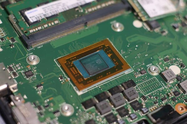
Not every consumer device needs the same board technology, and picking the wrong one either wastes money on unnecessary complexity or creates a product that physically can't be built the way it was designed. The right starting question isn't "what's the most advanced PCB technology" but "what does this specific device actually need to survive and fit."
| PCB Type | Typical Consumer Devices | Key Advantage |
|---|---|---|
| Single-sided | Remote controls, simple toys, basic chargers | Lowest cost, simplest to manufacture |
| Double-sided | Smart speakers, routers, small appliances | More routing room without a major cost jump |
| Multilayer | Laptops, TVs, gaming consoles | Handles complex circuits and higher power loads |
| Flexible | Wearables, cameras, foldable devices | Bends around curved or moving housings |
| Rigid-flex | Smartphones, foldable phones, smartwatches | Combines structural stability with flex routing in one assembly |
| HDI | Ultra-thin phones, wireless earbuds | Fits far more circuitry into a fraction of the space |
| RF / high-frequency | Wi-Fi routers, Bluetooth devices, 5G phones | Maintains signal integrity at high frequencies |
HDI boards are worth calling out specifically. Polaris Market Research notes that the HDI segment is projected to grow faster than any other PCB category, driven by rising demand for miniaturized, high-performance electronic products. That trend tracks with what's actually happening on store shelves: earbuds keep shrinking, phones keep getting thinner, and none of that is possible on standard-pitch boards.
How These Boards Actually Get Built
Manufacturing a consumer electronics PCB follows a defined sequence, and skipping steps or rushing quality checks is exactly where mass-produced electronics tend to fail in the field rather than in testing.
Design verification and DFM review: Before fabrication starts, the design files get checked against manufacturability rules, trace widths, hole sizes, and clearances, so early rework happens on a screen instead of at the factory.
Material selection and lamination: Copper-clad laminate layers are cut, stacked, and pressed under heat to form the board's core structure, with layer count and material chosen based on the device's electrical and thermal needs.
Circuit imaging and etching: A photoresist pattern defines the copper traces, and chemical etching removes everything else, leaving the actual circuit pathways behind.
Drilling and plating: Holes for vias and component leads are drilled, then plated with copper to create electrical connections between layers, including any blind or buried vias needed for dense layouts.
Solder mask and surface finish: A protective solder mask is applied, followed by a surface finish (ENIG, OSP, or immersion silver are common choices) that protects exposed copper and prepares pads for soldering.
Component assembly: Surface-mount and through-hole components are placed and soldered, typically using reflow ovens for SMT work on the tight tolerances consumer boards demand.
Inspection and testing: Automated optical inspection and, for dense or hidden connections, X-ray inspection catch defects before boards ship, since a visual pass alone can't confirm hidden solder joints.
Why These Boards Are Hard to Get Right
The volume and price pressure that define consumer electronics also create a specific set of manufacturing headaches that don't show up the same way in lower-volume industrial work.
Shrinking real estate: As devices get thinner and smaller, component pitches and trace spacing keep tightening, leaving less margin for drilling or alignment error before yield starts dropping.
Thermal management in tiny enclosures: Processors and batteries generate heat that has nowhere to go in a sealed, pocket-sized housing, forcing designers to route copper and place components with cooling in mind from the start.
Supply chain volatility: Component shortages and lead-time swings hit consumer electronics harder than niche industries simply because the order volumes are so much larger; a shortage on one part can delay a product launch by months.
Cost pressure at scale: Every added layer, finish option, or tighter tolerance multiplies across production runs in the tens of thousands, so design choices that seem minor on paper carry real budget weight in mass production.
Consistent quality across high volume: Catching a defect rate of even half a percent matters far more when a run is 100,000 units instead of 100, which is why inspection processes have to scale without slowing throughput.
Where the Technology Is Headed
The next few years of consumer electronics PCB development are being shaped less by new materials and more by how much smaller and smarter devices need to become without losing reliability.
Deeper HDI adoption: As microvia technology matures, more mainstream devices, not just flagship phones, are expected to adopt HDI construction to fit growing feature sets into shrinking housings.
Flexible and stretchable circuits expanding beyond wearables: What started in smartwatches is moving into foldable phones, health patches, and even clothing-integrated electronics.
Sustainability pressure on materials and processes: Halogen-free laminates and lead-free processes are shifting from a compliance checkbox to a genuine design consideration as environmental regulations tighten globally.
AI-assisted design and inspection: Automated DFM checking and AI-driven optical inspection are cutting the time between design submission and catching a manufacturability issue, which matters most in an industry where product cycles are measured in months, not years.
Faster prototype-to-production cycles: As consumer product launches compress, manufacturers are under growing pressure to cut the gap between a working prototype and a shippable production run.
How PCBgogo Supports Consumer Electronics Manufacturing
The technical demands above, tight layer stacks, fine-pitch vias, and finishes that hold up over years of handling, map directly onto what a consumer electronics PCB manufacturer needs to deliver consistently, not just occasionally.
Miniaturization support: PCBgogo fabricates boards up to 40 layers with blind, buried, via-in-pad, and laser-drilled microvias down to 3 to 6 mil, the kind of construction that lets a wireless earbud or ultra-thin phone board fit everything it needs to.
Material and finish flexibility: Boards are built on Shengyi and Kingboard laminates with a choice of ENIG, OSP, immersion silver, chemical tin, or gold-finger plating, so the finish matches the device's durability and handling requirements rather than a one-size-fits-all default.
Built-in quality verification: Every order goes through automated optical inspection and X-ray inspection, catching hidden defects on dense, multilayer boards before they reach assembly.
Per-order DFM review: An engineer reviews each design for manufacturability before production starts, which is exactly the kind of early check that keeps a consumer electronics launch on schedule instead of stuck in respins.
Fabrication and assembly under one roof: As an in-house factory handling everything from prototype through PCBA, PCBgogo removes the coordination gap between separate fabrication and assembly vendors, with prototypes typically ready in 1 to 3 days and assembled boards in 3 to 4 days for most builds.
Anyone scoping a new consumer electronics board can get an instant quote through PCBgogo's online tool to see turnaround and specs for their specific layer count and finish.
The Bottom Line
A consumer electronics PCB succeeds or fails on the same three axes every time: does it fit, does it survive daily use, and does it stay affordable at scale. Getting all three right starts with matching the board technology to the device and picking a manufacturing partner that can verify the design before it ever reaches production. From there, PCBgogo's online quoting tool is the fastest way to see what a specific layer count, finish, and turnaround will actually cost.
Consumer Electronics PCB: Frequently Asked Questions
What is the difference between a consumer electronics PCB and an industrial PCB?
Consumer electronics PCBs are optimized for compact size and low unit cost at high production volumes, while industrial PCBs typically prioritize extreme durability and long service life over size or price. Industrial boards can tolerate a larger footprint since they're rarely handheld, whereas consumer boards almost always have to fit a tight, portable enclosure.
How many layers does a typical consumer electronics PCB have?
It varies widely by device: simple appliances often use 2-layer boards, while smartphones and laptops commonly use 8 to 14 layers or more to fit dense circuitry into a small footprint. Ultra-compact devices like wireless earbuds sometimes push into HDI constructions with even finer stacking to save space.
Why do wearables use flexible or rigid-flex PCBs instead of rigid boards?
Wearables need to bend around curved surfaces like a wrist or fit into irregularly shaped housings, which a rigid board simply can't do without adding bulky connectors. Rigid-flex boards solve this by combining flexible sections for routing with rigid sections for mounting components, all in a single assembly.
What surface finish is best for a consumer electronics PCB?
It depends on the device's exposure and budget: ENIG offers strong durability and a flat surface good for fine-pitch components, while OSP is more cost-effective for boards that will be assembled quickly after fabrication. Devices with gold-finger connectors, like memory cards, typically need electrolytic or hard gold plating instead.
How long does it take to get a consumer electronics PCB prototype made?
Standard PCB prototypes are commonly ready in a few days once the design passes DFM checks, though exact timing depends on layer count and any advanced features like blind or buried vias. Assembled prototypes (PCBA) generally take a bit longer since component sourcing and soldering add steps after the bare board is finished.
Can one PCB manufacturer handle both fabrication and assembly for consumer electronics?
Yes, many manufacturers now offer one-stop fabrication and assembly services, which cuts out the coordination delays that come from shipping bare boards between separate vendors. This is especially useful for consumer electronics projects where tight launch timelines don't leave much room for handoff delays.





