




 日本語
日本語
 한국어
한국어

Cheap Keyboard PCB vs Premium PCB: A Selection Guide for Gaming Keyboard PCBs
QUICK ANSWER A cheap keyboard PCB can be the right choice for a proven wired layout with limited lighting and a fixed feature set. A premium PCB becomes worthwhile when a game keyboard needs low latency, hot-swap sockets, per-key RGB, wireless functions, tighter mechanical fit, controlled USB routing, and broader production testing.
Key Takeaways
Choose by risk, not price alone: A lower board quote can create higher total cost if connector failures, socket lift, rework, or inconsistent testing appear after launch.
Match the stackup to the feature set: Two layers can support a straightforward wired matrix. Four layers provide cleaner return paths when USB, dense RGB, wireless circuits, or compact routing compete for space.
Specify what affects fit and reliability: Board thickness, finished copper, surface finish, hole tolerance, outline tolerance, connector support, and test coverage should appear in the request for quotation.
Treat assembly as part of PCB design: Diode polarity, LED orientation, hot swap socket footprint, stencil openings, programming access, and test points determine whether a sound schematic becomes a repeatable product.
Introduction
Two keyboard PCBs may look almost identical in a product photo, yet behave very differently after thousands of key presses, repeated cable insertions, and full brightness RGB operation. The purchase decision is therefore less about a cheap label or a premium label and more about whether the board is engineered and tested for the intended game keyboard.
This guide compares the markets, applications, materials, fabrication controls, component assembly, and validation work behind each option. It also provides a practical selection process that a keyboard brand, designer, or purchasing team can use before requesting a quotation.
What Is a Keyboard PCB
A keyboard PCB is the electrical platform that connects every switch to a controller through a key matrix and sends the resulting input to a computer. Rows and columns reduce the number of controller pins needed, while one diode per switch can prevent unintended current paths when several keys are pressed together.
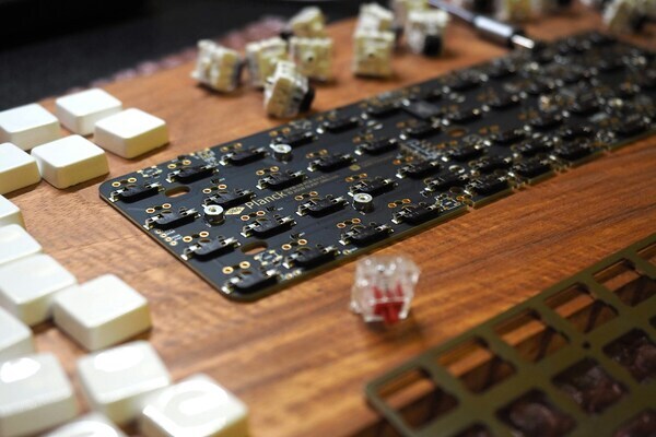
A basic board may contain a controller, USB connector, diodes, passive parts, and switch footprints. A more complex game keyboard can add hot-swap sockets, per-key RGB LEDs, rotary encoders, a display, wireless radio, battery charging, daughterboards, and firmware storage. USB 2.0 full speed operates at 12 Mbit/s, and its D+ and D- pair is normally designed around a 90 ohm differential target. That electrical requirement matters even though the keyboard data payload itself is small.
Markets for Cheap and Premium Mechanical Keyboard PCBs
Cheap mechanical keyboard PCBs serve price-sensitive products with stable layouts, modest feature counts, and predictable production volumes. Common targets include entry-level wired keyboards, office models, educational products, promotional devices, and private label boards based on a mature reference design.
The premium market serves esports products, enthusiast keyboards, compact custom layouts, creator controls, magnetic switch designs, and devices that need long-term firmware support. Buyers in this segment expect consistent sockets, uniform lighting, reliable USB behavior, useful remapping, and clean fit inside a carefully tuned case.
Applications for Cheap and Premium Mechanical Keyboard PCBs
Application complexity determines where added PCB cost produces a measurable benefit. The following examples show how features change the manufacturing and validation burden.
Standard wired keyboard: A two-layer board is often practical when the matrix, USB interface, and enclosure are already validated. The design should still include ESD protection near the external connector and accessible test points for power, ground, and matrix checks.
Per key RGB game keyboard: A full-size board may contain more than 100 LEDs. Power distribution, voltage drop, LED orientation, heat during reflow, and full brightness current testing become more important than the layer count alone.
Hot-swap enthusiast keyboard: The socket transfers insertion force into its solder joints and pads. Footprint accuracy, adequate copper anchoring, plate alignment, and controlled rework are essential because a lifted pad can disable a key position.
Wireless game keyboard: The PCB must separate noisy switching currents from the radio area, keep copper away from the antenna clearance defined by the module supplier, and manage battery charging safely. Enclosure material and nearby metal can also affect antenna performance.
Magnetic switch keyboard: Hall sensors measure magnetic field rather than a simple contact closure. Sensor placement, supply stability, calibration data, magnet orientation, and mechanical travel tolerances all influence actuation consistency.
Once these application demands are clear, the useful comparison moves from retail positioning to specific board and process choices.
Cheap Keyboard PCB vs Premium PCB Comparison
The practical difference between a cheap keyboard PCB and a premium PCB is the amount of design margin, process control, and verification assigned to critical functions. This table summarizes the purchasing implications.
| Decision area | Cheap keyboard PCB | Premium keyboard PCB | What to verify |
|---|---|---|---|
| Layer structure | Usually 2 layers for a proven matrix | Often 4 layers when routing density or return paths require it | Approved stackup and reference planes |
| Base material | General purpose FR 4 | FR 4 selected for thickness stability and process needs | Material family, thickness, Tg, and tolerance |
| Copper | Common finished copper specification | Copper selected for current and durability targets | Finished copper, not starting foil only |
| Surface finish | HASL may suit larger pads | ENIG can improve flatness for fine pads | Finish compatibility and storage plan |
| Signal control | Routing checked by standard design rules | Critical USB routing reviewed against the stackup | Target impedance and coupon requirement |
| Assembly | Standard placement and sampling | Tighter process review for dense LEDs and connectors | Stencil, polarity, first article, and reflow plan |
| Testing | Electrical test plus limited functional checks | Broader matrix, lighting, USB, and programming tests | Written test procedure and pass criteria |
How to Choose a Mechanical Keyboard PCB
The right mechanical keyboard PCB is the lowest risk design that meets the product requirements without paying for unused capability. Start with a written product specification, then convert each user-facing feature into an electrical, mechanical, manufacturing, or test requirement.
Define the input system: Record the key count, layout, rollover requirement, target polling behavior, switch technology, encoder inputs, and firmware update method. Confirm that matrix scan time and debounce settings support the claimed response behavior.
Calculate the power budget: List the maximum LED current, controller load, radio load, display load, and charging current. Check voltage drop at the farthest LEDs and confirm that the USB source or battery architecture can supply the chosen operating mode.
Lock the mechanical data: Release the PCB outline, mounting holes, plate drawing, stabilizer type, socket model, connector position, keepout zones, and height limits together. A 1.6 mm nominal PCB is common, but the actual product should use the thickness and tolerance required by its sockets and enclosure.
Plan verification before layout release: Provide test pads for power rails, USB access, matrix rows and columns, reset, and programming. Define whether the factory will run bare board electrical test, automated optical inspection, firmware programming, and a full key and lighting function test.
Compare complete cost: Include fabrication, components, stencil, assembly, programming, test fixtures, rework allowance, yield risk, packaging, and schedule. The meaningful figure is cost per accepted assembly, not the cheapest bare board line item.
This specification also gives the manufacturer enough context to suggest practical changes before tooling and component purchasing begin.
How PCBgogo Supports Premium Keyboard PCB Production
Premium keyboard production needs one controlled workflow from fabrication data through assembled board testing. PCBgogo can review the supplied Gerber data, bill of materials, placement file, assembly drawing, stackup request, impedance notes, firmware, and test instructions as one manufacturing package.
Materials and stackup: The engineering review can align the layer structure, board thickness, copper requirement, surface finish, and routing constraints with the design intent. For USB routing, impedance must be tied to the actual stackup rather than copied from a generic trace width.
Complex fabrication details: Keyboard projects may combine long board outlines, dense switch footprints, narrow solder mask features, connector cutouts, plated holes, and routing near the enclosure edge. Design for manufacturing feedback helps identify spacing, annular ring, outline, and panelization risks before production.
Impedance control: When controlled impedance is specified, the fabricator needs the target value, tolerance, reference layer, copper weight, dielectric structure, and the nets that require control. A coupon and measurement report should be requested when traceable impedance verification is part of acceptance.
Component placement: Assembly planning should address LED and diode polarity, hot swap socket orientation, USB connector support, fine pitch controller packages, moisture sensitive parts, stencil openings, and mixed SMT and through-hole steps. First article inspection is valuable before the full quantity proceeds.
Functional testing: A useful keyboard test checks every switch position, required key combinations, lighting channels, USB enumeration, current consumption, firmware version, and optional controls. The customer should provide the test sequence and acceptance limits so results remain repeatable across batches.
PCBgogo - Reliable, High-Quality PCB Manufacturing
Save time and money with an all-in-one solution for PCB fabrication, assembly, and parts. Reduce vendor coordination, avoid split shipments, and get consistent, reliable quality.
Get Free Quote >
Why PCBgogo Is a Strong Manufacturing Partner for Premium Keyboard PCBs
PCBgogo is a strong fit for premium keyboard PCB projects when the goal is to coordinate fabrication, sourcing, assembly, and testing through one accountable workflow. That structure reduces handoffs between separate suppliers and makes it easier to trace a problem to the design file, bare board, component, soldering process, firmware, or test method.
Quality depends on documented requirements and evidence. Bare board electrical testing, solder paste inspection where applicable, automated optical inspection, appropriate inspection for hidden joints, first article review, and product-specific functional testing address different failure modes. No single inspection replaces the others, and the required combination should be agreed before production.
Delivery speed improves when engineering questions are resolved before materials are committed. A complete data package lets PCBgogo review manufacturability, identify bill of materials conflicts, confirm assembly orientation, and prepare testing without waiting for missing files. Customers also gain a clearer communication path for engineering feedback, order status, exceptions, and corrective action.
Conclusion
Cheap Keyboard PCB vs Premium PCB is a decision about feature complexity, failure cost, and verification depth rather than price alone. Use a proven two-layer design for a straightforward product, and invest in stronger stackup planning, assembly control, and functional testing when a game keyboard adds dense lighting, hot-swap sockets, wireless hardware, magnetic sensing, or demanding mechanical packaging. Send PCBgogo a complete design and test package to obtain a manufacturing review based on the product you actually intend to ship.
Frequently Asked Questions
Is a cheap keyboard PCB always less reliable
No. A mature two-layer design can be reliable when its materials, mechanical dimensions, soldering, and tests are controlled. Reliability falls when cost reduction removes protection, weakens pads, changes approved components, or reduces test coverage without validation.
Does every game keyboard need a four-layer PCB?
No. A simple wired matrix can work well on two layers. Four layers become useful when dense routing, USB return paths, RGB power distribution, radio circuits, or compact packaging make a continuous ground reference difficult to maintain.
Which surface finish works for a keyboard PCB
HASL can suit many conventional pads, while ENIG provides a flatter surface that can help with smaller or more demanding land patterns. The correct choice depends on component geometry, assembly process, storage, cost, and the approved fabrication specification.
What should be tested on a hot-swap keyboard PCB?
Test every key position, the matrix combinations required by the product, USB connection, lighting, optional controls, and current draw. Mechanical inspection should also confirm socket alignment, plate fit, connector location, and that insertion force does not flex unsupported areas.
What files are needed for a keyboard PCBA quotation
Provide fabrication data, drill files, board drawing, bill of materials, placement coordinates, assembly drawings, stackup and impedance notes, approved substitutions, firmware, programming instructions, and the functional test procedure. Mechanical drawings for the plate and enclosure help expose fit risks early.





