
Castellated PCB Design & Manufacturing Guide
To create reliable castellated PCBs, designers must follow precise half-hole layouts, correct PCB edge plating design, and manufacturable drilling and assembly practices—this guide shows exactly how to do it.
What is a Castellated PCB?
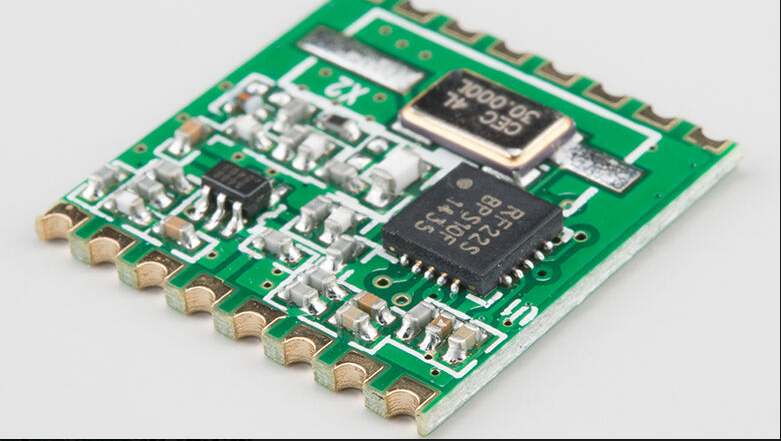
Castellated PCBs, also known as half-hole PCBs, are specialized printed circuit boards that feature plated edge connections along the board perimeter. These “castellations” enable modular designs, making it easy to integrate the PCB into larger assemblies or to connect multiple boards. They are widely used in IoT devices, modular electronics, and high-density PCB applications.
Understanding castellated PCB design is crucial for both functionality and manufacturability. Poor design can result in misaligned edge plating, insufficient mechanical strength, or even electrical connectivity issues. Therefore, collaboration between PCB designers and manufacturers is essential to ensure a high-quality product.
Key Principles of Castellated PCB Design
Edge Plating and Half-Hole Layout
The core feature of a half-hole PCB is its edge plating design. These half-hole PCBs require precise placement of plated holes along the edges of the board. The edge plating connects copper pads to the exposed half-holes, enabling reliable electrical and mechanical connections when soldered to another PCB.
When designing a castellated PCB, the half-hole diameter and spacing must match the manufacturing capabilities of the PCB fabricator. Typical designs use half-hole diameters ranging from 0.2 mm to 0.5 mm. Too small a hole may exceed the tolerances of standard drilling or laser drilling processes, while too large a hole can weaken the mechanical integrity of the edge plating.
Board Layout and Mechanical Considerations
Castellated PCB design requires careful attention to both electrical and mechanical layout. Designers must ensure that signal traces leading to the half-holes do not compromise edge plating integrity. Additionally, copper clearance and pad size should be sufficient to allow for reliable soldering and prevent short circuits.
Including fillets or chamfers along the edge can improve the robustness of the board during assembly. Most manufacturers recommend a chamfer radius between 0.5 mm and 1 mm to reduce edge stress and improve solderability.
Design for Manufacturability (DFM)
One of the most critical steps in castellated PCB design is incorporating manufacturability considerations. This includes:
Minimum pad-to-pad spacing to prevent solder bridging
Drill tolerances compatible with mechanical or laser drilling
Controlled copper plating thickness for half-holes to ensure consistent electrical conductivity
Collaboration with the PCB manufacturer during the design stage ensures that the board can be reliably fabricated without costly revisions or production delays.
Manufacturing Processes for Castellated PCBs
Drilling Techniques: Mechanical vs. Laser
Half-hole PCBs can be fabricated using either mechanical drilling or laser drilling. Mechanical drilling is cost-effective for larger holes but may struggle with diameters below 0.3 mm. Laser drilling provides high precision, capable of creating holes as small as 0.2 mm, and is ideal for high-density castellated PCBs.
Manufacturers often provide detailed specifications, including the minimum hole diameter and tolerance, to guide the design process and prevent alignment issues during production.
PCB Edge Plating Process
The edge plating process is essential for half-hole PCBs. After drilling, the board undergoes electroless copper deposition followed by electroplating to create a uniform copper layer along the edges. This ensures electrical connectivity and mechanical strength for modular assembly.
Key factors in PCB edge plating design include pad size, plating thickness, and copper coverage. Properly plated edges reduce the risk of weak solder joints and improve the overall reliability of the PCB.
Soldering and Assembly Considerations
Castellated PCBs are designed to be soldered onto host boards or modules. Ensuring proper half-hole alignment and pad design during assembly is critical. Automated assembly processes, including pick-and-place and reflow soldering, can be used to achieve consistent results.
During manufacturing, quality control measures such as Automated Optical Inspection (AOI) and X-ray inspection are applied to verify hole dimensions, copper plating, and solderability. This ensures the final product meets design specifications and maintains reliable electrical connections.
Quality Control for Castellated PCBs
Dimensional Inspection
Accurate measurement of half-hole diameter, pad size, and spacing is essential. Dimensional inspection ensures that the castellations will fit precisely when integrated into larger assemblies or modules.
Plating and Conductivity Verification
The copper plating of the half-holes must be continuous and uniform. X-ray inspection or cross-sectional analysis can verify plating thickness and identify any voids or defects. Maintaining consistent conductivity across all half-holes is critical for electrical reliability.
Mechanical and Thermal Testing
Castellated PCBs often face mechanical stress during assembly. Thermal cycling and solder pull tests are used to confirm the robustness of the edge plating and half-holes. This step ensures that the PCB can withstand real-world operational conditions without failures.
Why Choose PCBGOGO to Manufacture Your Castellated PCBs?
Advanced Equipment for Precision Fabrication
PCBGOGO offers CNC and laser drilling capabilities that support high-density half-hole PCBs. With edge plating precision up to ±0.05 mm, we can produce complex castellated designs with consistent quality.
Design Support and Review
Our engineers provide detailed reviews of castellated PCB designs, including half-hole placement, PCB edge plating design, and pad layout. This helps identify potential manufacturing issues before production, reducing iterations and ensuring manufacturability.
Comprehensive Quality Assurance
We employ AOI and X-ray inspection systems to verify half-hole dimensions, plating quality, and solderability. Each batch undergoes sampling for solder pull and thermal testing, ensuring that every board meets high standards of reliability.
FAQ: Common Questions About Castellated PCBs
Q: What is the minimum half-hole size supported?
A: PCBGOGO supports half-holes as small as 0.3 mm.
Q: How is PCB edge plating achieved?
A: Electroless copper deposition followed by electroplating creates uniform conductive edges.
Q: Can castellated PCBs be integrated into modular boards?
A: Yes, properly designed half-holes allow easy soldering and mechanical connection to host PCBs.
Q: What design factors improve manufacturability?
A: Correct hole diameter, pad size, spacing, and chamfered edges all contribute to reliable fabrication.
Conclusion
Castellated PCBs, or half-hole PCBs, are key components in modular electronics and high-density PCB applications. Proper castellated PCB design, careful PCB edge plating design, and adherence to manufacturing capabilities are essential for creating functional and reliable boards. By integrating design and manufacturing considerations from the beginning and partnering with experienced fabricators like PCBGOGO, designers can ensure their castellated PCBs are high-quality, precise, and ready for integration into larger systems. Contact PCBGOGO experts to get a professional guide in PCB design and manufacturing.

