




 日本語
日本語
 한국어
한국어

Board-to-Board PCB Connector Selection and Layout Guide
A board-to-board PCB connector joins two printed circuit boards through a matched pair of contacts. Choose it by board orientation, mated height, pin count, electrical load, and the conditions in which the assembly will operate. Then check both part drawings, the complete PCB stack, and a physical prototype. Pitch alone cannot establish compatibility or reliability.
A compact enclosure can make two boards look easy to stack on screen, yet a mounting boss may prevent the first prototype from mating. Connector choice belongs in the mechanical design before either PCB footprint is frozen.
What Is a Board to Board PCB Connector
A board-to-board PCB connector is a separable electrical interface between two circuit boards. Its two mating parts are normally mounted on different PCBs, so power and signals can cross between them without a loose wire harness. The connection may be permanent for the life of the product or opened during assembly and service.
The connector is a system, not a single part number. The plug and receptacle must be an approved mating pair with compatible contact count, pitch, orientation, plating, and mated height. A PCB card edge that plugs into a socket is another board connection, but the finished edge needs its own thickness, bevel, and plating controls.
Before searching a catalog, sketch the installed boards. Mark mating direction, board separation, enclosure walls, fasteners, and nearby components.
Which Connector Type Fits the Board Arrangement
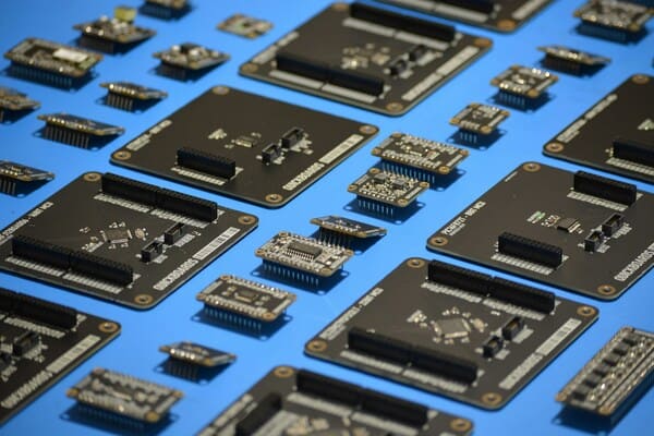
Board arrangement determines the connector family before pitch or pin count does. The table compares common options by their actual mechanical relationship.
| Connector type | Board arrangement | Typical reason to choose it | Design check |
|---|---|---|---|
| Mezzanine or stacking pair | Parallel boards, one above the other | Dense connections in compact instruments or modules | Specified mated height and space for components between boards |
| Right angle or orthogonal pair | Boards meet at 90 degrees | Daughtercards and modular control boards | Insertion path, edge position, and support against leverage |
| Coplanar pair | Boards sit side by side on roughly one plane | Modular boards with a narrow joint | In plane alignment and mechanical retention |
| Backplane connector | Plug in cards meet a shared board | Replaceable cards in a rack or chassis | Guides, insertion force, and the full signal channel |
| Pin header and socket | Usually parallel or perpendicular, depending on parts | Simple serviceable interconnects and prototypes | Retention, exposed contacts, and actual mating length |
| Card edge socket | A plated PCB edge inserts into a socket | Removable modules without a second soldered connector | Board thickness, finger finish, bevel, and key position |
A mezzanine connector suits a small sensor board stacked above a controller. A card edge can suit a sliding module, while a backplane system suits repeated card replacement.
How to Choose Pitch Height and Pin Count
Pitch, mated height, and pin count describe different constraints. Pitch is the center to center distance between neighboring contacts; mated height is the distance defined by the assembled connector pair. Neither measurement gives the whole three dimensional envelope.
Start with the board stack. Add the PCB thicknesses, spacers, soldered component heights, enclosure features, and tolerance of each item. Compare the resulting minimum and maximum separation with the connector family’s allowed mated range. Kyocera’s board-to-board selection guide shows parallel connector options from 0.6 mm to 26.0 mm stack height, which illustrates why a single nominal height cannot stand in for a specific mating pair. Use the selected part drawing for final dimensions.
Next, assign contacts to functions. Count signal lines, grounds, supply pins, and any pins reserved for identification or future revision. For a high speed link, ground contacts may be needed between or beside signal groups according to the connector maker’s pinout guidance. Do not treat unused contacts as automatic current capacity or connect parallel power pins without confirming the manufacturer’s rules for current sharing and temperature rise.
Choose pitch after those requirements are known. A finer pitch saves contact row length but can tighten footprint tolerances and routing space. Compare actual 3D models and land patterns, then verify that an operator or fixture can mate the boards without tilting them.

How Electrical and Mechanical Ratings Affect Reliability
Electrical and mechanical ratings describe the conditions under which a connector is expected to work. Read them for the exact part and test conditions, especially when the design carries power, fast data, or repeated service cycles.
Current and voltage: Check current per contact, allowable temperature rise, contact resistance, and voltage rating. A power path also includes the PCB trace, via, solder joint, and any wire beyond the second board. The lowest capable element governs the path. Measure voltage drop and connector temperature in the assembled enclosure at the intended load.
Signal performance: A high speed connector should have characterization relevant to the required interface, but the board launch and return path remain part of the channel. Route differential pairs and nearby grounds using the chosen connector’s guidance. Excessive stubs, split return planes, or an abrupt transition can spoil a link even when the connector itself has a suitable data rating.
Retention and mating cycles: Check whether the pair uses friction, a latch, screws, or chassis guidance, and compare its durability rating with expected use. A factory mated connector has a different job from a monthly service module. Support the board so solder joints do not carry repeated insertion force.
Environment: Review operating temperature, vibration, shock, contact finish, and contamination exposure as a system. A gold finish does not compensate for poor board support. Validate the complete assembly under the application’s vibration conditions.
PCB Layout Rules for a Reliable Mating Pair
A reliable PCB layout positions both connector halves from the same mechanical references and preserves the manufacturer’s footprint. The connector cannot correct a board outline or mounting pattern that puts the two halves in different locations.
First, place the footprints using the mating drawings, not two independent visual guesses. Confirm pin 1 from the same viewing direction on both boards, then compare the 3D assembly. If two connectors mate at once, evaluate the accumulated position tolerance between them. Samtec describes a floating board-to-board family with 0.50 mm of X movement and 0.20 mm of Y movement for alignment error, but that allowance belongs only to that family. Do not transfer its numbers to a rigid connector.
Second, reserve the full insertion and removal path. Tall components, shield cans, screw heads, and enclosure ribs can block straight mating or prevent a latch from opening. Keep the connector maker’s local keepout, solder mask, stencil, and panel edge instructions visible in the fabrication and assembly data. Check the finished board thickness where a card edge or press fit contact depends on it.
Third, support the boards close enough to the interface that mating force does not bow the PCB. For example, Molex’s Mirror Mezz application specification recommends standoffs within 30 mm of every connector corner and a standoff length matched to mated height within 0.15 mm. Those are product specific instructions, not a universal rule. The broader lesson is to design support around the chosen connector instead of relying on solder joints to hold a board stack together.
Finally, make the electrical path inspectable. Keep ground continuity through the connector, place test points where practical, and document power pin assignments. Review copper width, via count, and return path on both boards together.
Assembly and Prototype Checks Before Production
Prototype validation should test the complete mated assembly, because a continuity check on bare PCBs cannot reveal a blocked insertion path or an unstable contact under load. Use this sequence before releasing the design.
1. Verify the exact mating part numbers, footprints, pin maps, and polarity in the bill of materials and assembly drawings.
2. Inspect the first built boards for solder bridging, poor wetting, bent contacts, housing damage, and connector tilt. For fine pitch parts, check the manufacturer’s reflow and stencil guidance.
3. Mate the boards in the actual enclosure with the intended screws or guides. Confirm full seating without forcing one corner, and check clearance during removal.
4. Measure continuity, voltage drop, and temperature at operating load. For high speed interfaces, run the relevant link or channel test rather than relying on continuity alone.
5. Repeat the intended service cycle and environmental tests when the product will see frequent mating, vibration, or thermal movement.
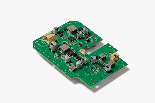
At the manufacturing stage, the footprint and placement data should agree with the mechanical drawing and the selected connector package. PCBgogo supports SMT, through hole, and mixed PCB assembly, along with design file review and inspection. That combination is relevant when a board pairs a fine pitch mezzanine connector with mechanically anchored through hole parts. Send the exact connector drawings and assembly notes with the PCB files so the build can be checked against the actual mating system.
Common Connector Problems and What to Check
Connector failures are easier to diagnose when the electrical symptom is tied back to the board stack and assembly process. The table gives starting checks; measurements on the finished product still determine the cause.
| Symptom | First checks | Likely design response |
|---|---|---|
| Boards do not fully seat | Wrong mating pair, blocked keepout, incorrect spacer height, tilted connector | Recheck drawings and stack dimensions; correct interference before applying force |
| Intermittent signals when the unit moves | Incomplete seating, board flex, damaged contacts, cracked solder joint | Add support or retention and inspect both halves under movement |
| Warm connector at normal load | Contact resistance, current assignment, partial mating, undersized copper | Measure drop and temperature; review the complete current path |
| High speed link passes continuity but fails data test | Poor launch, broken return path, excess stub, wrong pin assignment | Review both PCB layouts and test the complete channel |
| Mating damages pads or housing | Misalignment, excessive insertion force, missing guides | Improve board guidance and local mechanical support |
Fix the geometric or electrical cause, then build another prototype. Forcing a misaligned pair can hide the original fault while reducing connector life.
Frequently Asked Questions
Are board to board connectors interchangeable if they have the same pitch
No. Matching pitch does not guarantee compatible contact shape, body geometry, pin count, plating, or mated height. Select the approved mating part listed by the manufacturer and check both drawings.
How do I calculate the correct board stack height
Start with the installed distance between the two PCB mounting surfaces, then account for board thickness, spacers, and component clearance. Compare the minimum and maximum toleranced separation with the chosen connector’s allowed mated height rather than using only the nominal enclosure dimension.
Can one board to board connector carry both power and high speed signals
Yes, if the selected connector family supports the required current and signal performance and its recommended pin assignment allows both. Verify power contact derating, ground allocation, and channel behavior in the finished layout. A generic signal connector rating does not establish the performance of the entire board pair.
Does a smaller pitch always make the PCB assembly smaller
No. The housing, board supports, mating access, routing area, and keepouts can control the final size. Compare the complete mated model in the enclosure before trading a larger connector for a finer pitch.
When should I choose a floating connector
A floating connector can help when two boards or multiple connector pairs have unavoidable alignment variation within the family’s stated movement limits. It does not replace a proper tolerance analysis, guides, or board support. Use the float values published for the exact pair.
Conclusion
Choose a board-to-board PCB connector as part of the mechanical and electrical system: define board orientation, stack tolerance, pin assignment, support, and test method before freezing the PCB layout. The most useful final check is a fully assembled prototype that mates cleanly and performs under realistic load. When preparing the build, include both connector drawings and clear assembly notes with the PCB files.





