日本語
 한국어

Blind and Buried Vias in HDI PCB Design
KEY DEFINITION A blind via connects an outer PCB layer to one or more inner layers without crossing the full board. A buried via connects internal layers only. Both increase HDI routing density and shorten interconnects, but they require tighter registration, controlled plating, and more manufacturing steps than a standard through via.
Fine-pitch BGAs, compact power stages, and dense processor boards often run out of routing channels before they run out of electrical connections. A blind via solves that problem selectively: it reaches only the layers the signal or power path needs, leaving the remaining layers available for routing.
The practical decision is not simply whether HDI is desirable. Designers must select the correct via structure, build a manufacturable stackup, protect signal return paths, and create a credible heat path from each thermal pad.
What Blind and Buried Vias Are
Blind via and buried via structures are depth-limited plated connections that reduce the layer area consumed by a full-depth hole.
What Is a Blind Via
A blind via starts on the top or bottom copper layer and terminates on an internal layer. It may be produced as a laser-drilled microvia for HDI work or, at larger dimensions, by controlled-depth mechanical drilling. The term describes the layers connected; it does not automatically define the hole diameter.
What Is a Buried Via
A buried via connects two or more internal layers and is invisible after final lamination. The fabricator drills and plates the relevant inner-layer subassembly before adding the outer layers. This creates routing freedom but adds at least one controlled sub-build and lamination dependency.
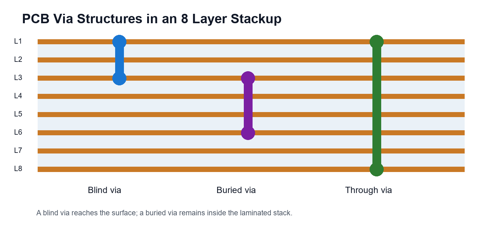
Blind Via and Buried Via Roles in HDI
In an HDI stackup, a blind via usually handles surface escape routing while a buried via carries selected connections within the core. A 1+N+1 build has one buildup layer on each side of an N-layer core; higher-order builds add more buildup and lamination cycles. Mixing short blind microvias with conventional through holes often gives a better balance of density, reliability, and cost than using HDI structures everywhere.
How Blind and Buried Vias Are Manufactured
Blind via manufacturing starts by matching the via span, dielectric thickness, and drilling method to the planned stackup.
Laser drilling: CO2 or UV systems create small, shallow blind via structures, normally between adjacent buildup layers. The hole is cleaned before electroless copper deposition and electrolytic plating.
Controlled-depth drilling: A mechanical drill stops at a specified depth for larger blind structures. Depth tolerance, copper thickness, and the risk of contacting the next layer must be reviewed together.
Filling and capping: Copper or resin filling followed by planarization and cap plating creates a flat via-in-pad surface. This prevents solder loss into the hole beneath a BGA or exposed thermal pad.
Sequential lamination: Buried vias are drilled and plated in an inner subassembly before the next layers are laminated. Each added buildup stage increases registration and process-control demands.
Microvia geometry also changes the risk profile. Staggered microvias land on offset pads and generally avoid a direct stress column. Stacked microvias align vertically and require reliable fill and bonding at every interface. Skip microvias cross more than one dielectric layer; they can simplify routing, but the deeper hole is harder to ablate, clean, and plate consistently.
Benefits and Limitations of a Blind Via
A blind via is most valuable when it removes a specific routing, signal-integrity, or packaging constraint.
| Design effect | Practical benefit | Tradeoff to control |
|---|---|---|
| Blind via BGA escape | More routing channels remain below unused layers | Smaller capture pads increase registration sensitivity |
| Short vertical transition | Less unused barrel and lower via-stub resonance | Return-path continuity still needs nearby ground transitions |
| Via in thermal pad | A short path can move heat into internal copper planes | Open holes can wick solder and should be filled and capped when required |
| Selective layer access | Outer layers remain available for placement and routing | Sequential lamination raises process complexity and lead time |
For thermal management, distinguish an electrical blind via from a thermal via array. A blind via in or near a thermal pad can shorten the heat path to an internal copper plane, but the full thermal path also depends on copper area, via fill, laminate conductivity, airflow, and the final heat sink or chassis. Thermal management must therefore be verified at board and enclosure level, not inferred from via count alone.
Reliability and Common Failure Modes
Blind via reliability depends on clean target-pad bonding, complete plating, accurate registration, and a structure that tolerates assembly and service temperatures.
Target-pad separation: A weak interface at the base of a blind via can open after reflow or thermal cycling.
Voids and copper cracks: Incomplete blind via cleaning or plating can leave thin regions that concentrate current and mechanical strain.
CTE-driven stress: Copper and laminate expand differently through the board thickness, so repeated heating loads the via barrel and interfaces.
Stacked-microvia fatigue: A vertical stack transfers stress through several plated interfaces; staggered construction may be preferable when routing permits.
A suitable qualification plan can combine microsectioning, electrical continuity testing, X-ray inspection for filled structures, and thermal stress testing. IPC-2226 provides HDI design guidance, IPC-6012 defines performance requirements for rigid printed boards, IPC-A-600 covers visual acceptance, and IPC-TM-650 contains applicable test methods. The procurement drawing should state the required class and acceptance criteria rather than naming a standard without a measurable requirement.
Key Blind Via Design Guidelines
Reliable design begins by treating the blind via and stackup as one manufacturing system.
Control blind via depth and aspect ratio: Select dielectric thickness and finished hole size together. A shallow geometry is easier to clean and plate; the approved limit must come from the chosen fabricator and material set.
Position the blind via capture pad deliberately: Allow for layer registration, laser alignment, annular ring, and copper-feature spacing. Do not place a blind via only from nominal CAD geometry.
Plan every via span before routing: Define blind, buried, and through drill pairs in the stackup drawing. Minimizing unique spans reduces process steps and CAM ambiguity.
Protect signal and power integrity: Keep the signal transition short, provide an adjacent reference plane, and place ground vias close enough to support return current. For power, check current density and DC resistance instead of assuming that several small vias equal one large via.
Design the thermal pad as a solder and heat structure: Specify whether vias under the thermal pad are filled, capped, or tented. Filled and capped via-in-pad supports a flat solder surface and a controlled thermal management path.
When to Use Each PCB Via Type
Choose the simplest via that meets routing, electrical, thermal, and assembly requirements.
| Design condition | Preferred starting point | Reason |
|---|---|---|
| Standard multilayer board with adequate routing space | Through via | Lowest process complexity and broadest fabrication window |
| Fine-pitch BGA or dense outer-layer escape | Blind microvia | Reaches a nearby routing layer without blocking the full stack |
| Internal routing must avoid consuming surface area | Buried via | Connects core layers while leaving both surfaces clear |
| High-speed thick board with a harmful unused stub | Back-drilled through via | Removes the stub without converting the whole design to HDI |
| Exposed thermal pad under a power package | Filled and capped via-in-pad or qualified thermal via array | Controls solder while connecting the pad to a heat-spreading plane |
Avoid blind and buried vias when ordinary through vias meet density and performance targets, when the fabricator cannot confirm the proposed stackup, or when the program cannot absorb the additional lamination, inspection, and qualification work.
PCBgogo Expertise in Blind Via HDI Production
A blind via design is production-ready only when drilling, lamination, filling, imaging, and inspection capabilities are evaluated against the same stackup.
Laser and controlled-depth drilling: PCBgogo lists 0.10 mm as its production minimum for laser microvias, with 0.075 mm available for qualified prototype constructions after engineering review. Controlled-depth drilling is also available for larger blind mechanical structures.
Advanced HDI structures: PCBgogo supports blind and buried vias, sequential lamination, copper-filled microvias, resin-filled via-in-pad, and staggered or stacked structures. Published configurations include 1+N+1, 2+N+2, and 3+N+3, while more complex builds require engineering approval.
Design for manufacturing review: The review checks via depth and diameter, dielectric thickness, registration, copper distribution, fill requirements, and the complete drill map before release. This is especially important when a blind via sits inside a BGA land or thermal pad.
Process verification: Available controls include LDI and AOI for fine features, electrical testing for continuity, and inspection planning for filled vias and high-reliability HDI. The final quality plan should match the product's IPC class and service environment.
Frequently Asked Questions
What is the main difference between blind and buried vias?
A blind via connects an outer layer to one or more inner layers, while a buried via connects internal layers only. The buried structure is enclosed during lamination and cannot be seen on the finished board.
Is every blind via a microvia?
No. Blind via describes layer reach, while microvia describes a small HDI interconnect geometry. Many blind vias are laser microvias, but larger blind holes can be mechanically drilled.
Are blind and buried vias reliable?
Yes, when the geometry, materials, plating, and lamination process are qualified together. Blind via reliability risk rises with poor target-pad bonding, excessive depth-to-diameter ratio, misregistration, voids, or unnecessary stacked structures.
Why are buried vias more expensive?
A buried via must be drilled and plated before the outer layers are laminated. The added sub-build, lamination, alignment, and inspection steps increase manufacturing time and process risk.
Can a blind via connect multiple layers?
Yes, a blind via can terminate beyond the adjacent inner layer if the manufacturing process supports that span. Deeper structures are harder to drill, clean, and plate, so they need early fabricator approval.
When should back drilling be used instead?
Use back drilling when a through via is otherwise acceptable but its unused barrel creates a harmful high-speed stub. It is often more practical than redesigning the board around blind vias.
How does a blind via improve signal integrity?
A blind via can shorten the vertical transition and reduce or eliminate the unused via stub that causes resonance and impedance discontinuity. It still needs a continuous reference path and appropriate ground transitions.
Final Design Check
Use a blind via only after the stackup, via spans, thermal pad construction, signal return paths, and acceptance tests are defined. Send the complete stackup and drill map for DFM review before layout is frozen; this prevents a compact HDI concept from becoming an unreliable or unbuildable board.