日本語
 한국어

Analog and Digital Signals in Practical PCB Design
KEY TAKEAWAYS Analog and digital signals require different PCB layout priorities. Analog paths need low noise, short current loops, and careful reference integrity; digital paths need controlled return paths, impedance awareness, and edge rate management. Mixed-signal success depends on partitioning by current flow rather than splitting ground without a plan.
Introduction
A schematic can be electrically correct and still fail on the bench because the PCB changes waveform behavior. Copper geometry adds resistance, inductance, capacitance, coupling, and discontinuities that do not appear as ideal wires in a circuit diagram.
This guide explains analog vs. digital circuits through decisions PCB designers make every day: placement, return paths, layer stackup, routing, power integrity, verification, and preparation for production.
What Are Analog Signals
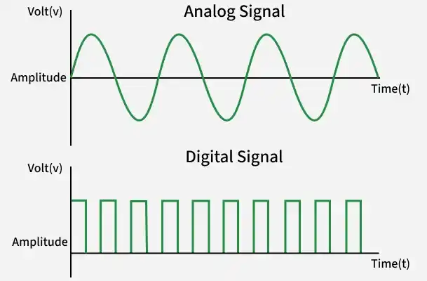
Analog signals vary continuously in amplitude over time. On a PCB, they carry real-world quantities such as sensor voltage, audio, or power feedback, so added noise or distortion directly changes the information.
What Are Digital Signals
Digital signals use discrete voltage levels to represent logic states such as 0 and 1. Their transitions are still analog waveforms, so edge rate, ringing, and return paths matter on a PCB.
Differences Between Analog and Digital Signals
The central difference between analog and digital signals is how noise becomes an error: analog error usually changes the measured value continuously, while digital error matters when noise or timing causes a receiver to choose the wrong logic state.
The table translates analog vs digital circuits into practical PCB consequences rather than abstract definitions.
| Design factor | Analog signals | Digital signals | PCB implication |
|---|---|---|---|
| Information | Continuous amplitude and timing | Discrete states sampled in time | Define the permitted amplitude or timing error |
| Main risk | Noise, gain, drift, offset and distortion | Threshold violation, jitter and false switching | Review both waveform quality and functional margin |
| Key property | Signal level, bandwidth and source impedance | Edge rate timing budget and interface impedance | Route from the electrical requirement, not the net name |
| Return current | Follows the lowest impedance loop for the signal frequency | Concentrates beneath fast traces on the nearest reference plane | Keep a continuous reference and avoid unintended loop area |
| Verification | Noise spectrum gain linearity and settling | Eye margin, overshoot timing and bit error behavior | Choose test points and probes before layout release |
Advantages and Disadvantages of Analog and Digital Signals
The advantages of each signal type depend on the function, noise environment, bandwidth, power budget, and conversion requirements of the product.
Analog strengths: Analog paths can preserve continuously varying information with low latency and may require little processing for sensing, amplification, filtering, or control.
Analog limits: They accumulate noise, offset, drift, and component tolerance errors. Long high-impedance routes and poor grounding can degrade accuracy before the signal reaches a converter.
Digital strengths: Digital data can be stored, processed, copied, checked, and transmitted with defined logic margins. Error detection can make communication resilient when the physical link is designed correctly.
Digital limits: Fast edges create broadband current demand and electromagnetic emissions. Dense buses also impose timing, impedance, crosstalk, and power distribution constraints.
Many products therefore combine both domains: analog circuitry acquires or drives a physical quantity, and digital circuitry processes, controls, or communicates the result.
Applications of Analog and Digital Signals
Both signal domains usually coexist because real-world inputs are continuous while control, storage, and communication are often digital.
Industrial sensing: A bridge sensor or thermocouple produces a small analog voltage, an amplifier and filter condition it, and an analog-to-digital converter passes samples to a microcontroller.
Motor control: Current shunts and position sensors create analog feedback while PWM outputs and control buses carry digital commands. High di dt switching loops must stay away from measurement paths.
Audio equipment: Microphone and line inputs remain analog until conversion, while digital signal processing handles filtering, mixing, and interfaces. Clock noise can couple into the analog output and create audible tones.
Power conversion: Feedback and current sense nodes are analog, while enable, telemetry, and supervisory links are digital. The switch node requires strict copper and spacing discipline.
Data acquisition: Multiple analog channels share references, converters, and power rails while digital buses transfer results. Channel isolation, settling time, and return current paths drive the layout.
PCB Design Guide for Analog Signal Circuits
A reliable analog PCB protects signal integrity by controlling current loops, reference quality, coupling, leakage, and component placement.
1. Place by signal flow: Put the connector, protection, conditioning, amplifier, filter, and converter in functional order. Place gain setting and feedback parts beside the relevant pins so their loops remain small.
2. Protect the reference: Use a solid reference plane under analog signals unless the circuit architecture requires isolation. Do not route a trace across a plane split because return current must detour, increasing loop area and coupling.
3. Separate noisy current loops: Keep DC-DC switch loops, gate drives, inductors, and high-current rectification paths compact and physically distant from low-level inputs. Separation should follow current flow, not cosmetic analog and digital labels.
4. Match impedance to sensitivity: Shorten high-impedance nodes first. Use guard copper only when its driving potential and leakage behavior are understood, and remove solder mask contamination risks where femtoamp or picoamp leakage matters.
5. Filter at the boundary: Place input protection and filtering close to the connector or receiving device. For an ADC, confirm the input network can settle within the acquisition interval rather than choosing an RC filter from cutoff frequency alone.
6. Plan measurement access: Provide ground-adjacent test points and probe locations that do not add long stubs. Validate noise with an appropriate probe connection because a long ground lead can display ringing created by the measurement setup.
Before release, review the complete tolerance chain: sensor error, resistor ratio, amplifier offset and bias current, reference accuracy, converter error, temperature drift, and PCB leakage. Layout cannot recover margin that the error budget never reserved.
PCB Design Guide for Digital Signal Circuits
A reliable digital PCB keeps each fast signal and its return current on a controlled path while maintaining timing and power integrity.
1. Design for edge rate: Use the driver rise time, not only the data rate, to judge transmission line behavior. If propagation delay becomes a meaningful fraction of rise time, model the interconnect and consider source or end termination.
2. Route over a continuous plane: Keep fast traces on a layer adjacent to an unbroken reference. When a signal changes reference planes, add a nearby stitching via or appropriate return path so high-frequency current does not spread across the board.
3. Control geometry: Set trace width and spacing from the actual stackup and copper thickness. Ask the fabricator to confirm controlled impedance values before final routing because generic field solver assumptions may not match production materials.
4. Limit crosstalk: Increase spacing, reduce parallel run length, keep aggressors away from board edges, and avoid routing fast signals beside sensitive analog nets. Spacing is usually more effective than adding a grounded guard trace without enough stitching vias.
5. Stabilize the power distribution network: Place small decoupling capacitors close to power pins with short connections to power and ground. Group bulk capacitance by load step and rail behavior, then check plane transitions, via inductance, and simultaneous switching demand.
6. Verify timing and topology: Apply interface-specific length matching only where the timing budget requires it. Match delay rather than visual trace length, and avoid excessive serpentine routing that increases coupling and loss.
Analog vs digital circuits converge at converters, mixed-signal ICs, connectors, and shared supplies. At these boundaries, follow the component pinout and reference recommendations, keep return paths continuous, and prevent digital currents from crossing the analog placement area.
From PCB Design Files to Reliable Production
Manufacturing quality matters because signal integrity depends on the fabricated stackup, copper geometry, drilling, soldering, component orientation, and assembly process matching the design intent. Release a complete package with Gerber or ODB data, drill files, stackup notes, impedance requirements, fabrication drawings, BOM, centroid data, assembly drawings, and test expectations as applicable.
If you need a custom analog signal PCB, digital signal PCB, or mixed signal PCB, contact PCBgogo. PCBgogo provides one-stop PCB fabrication and PCBA manufacturing support, helping move these projects from prototype through volume production with manufacturing equipment, controlled processes, and responsive service.
Before ordering, request a design for manufacturability review and resolve stackup, impedance, annular ring, solder mask, component availability, polarity, and testability questions. This handoff reduces avoidable revisions and gives the factory clear acceptance criteria.
Frequently Asked Questions
Can analog and digital signals share the same ground plane
Yes, they often should share a continuous ground plane when the return currents are controlled by placement and routing. A split plane can make both domains worse if a trace crosses the split and forces its return current around a long detour.
How far apart should analog and digital traces be
There is no universal distance because coupling depends on stackup, trace geometry, parallel length, edge rate, and victim sensitivity. First reduce parallel exposure and keep fast digital signals over a close reference plane, then use field solving or signal integrity analysis when margins are tight.
Does a low clock frequency mean signal integrity is unimportant
No. A low-frequency clock with fast edges can still ring, radiate, and create crosstalk. Base routing and termination decisions on transition time, interconnect delay, topology, and receiver thresholds.
Where should an ADC be placed on a mixed-signal PCB
Place the ADC at the boundary between the analog signal chain and digital processing area, with short analog inputs and a clean reference path. Route its digital interface away from the analog input network and follow the device recommendations for supplies, reference pins, and exposed pad grounding.
What files help a PCB manufacturer preserve signal integrity
Provide the layer stackup, controlled impedance requirements, copper weights, material constraints, fabrication data, drill files, drawings, and clear net or coupon requirements. For PCBA, also provide the BOM, centroid data, assembly drawings, polarity information, and test criteria.